- 您現(xiàn)在的位置:買賣IC網(wǎng) > PDF目錄299156 > GE28F640W30TD70 (INTEL CORP) 4M X 16 FLASH 1.8V PROM, 70 ns, PBGA56 PDF資料下載
參數(shù)資料
| 型號(hào): | GE28F640W30TD70 |
| 廠商: | INTEL CORP |
| 元件分類: | PROM |
| 英文描述: | 4M X 16 FLASH 1.8V PROM, 70 ns, PBGA56 |
| 封裝: | 0.75 MM PITCH, VFBGA-56 |
| 文件頁(yè)數(shù): | 59/104頁(yè) |
| 文件大小: | 1443K |
| 代理商: | GE28F640W30TD70 |
第1頁(yè)第2頁(yè)第3頁(yè)第4頁(yè)第5頁(yè)第6頁(yè)第7頁(yè)第8頁(yè)第9頁(yè)第10頁(yè)第11頁(yè)第12頁(yè)第13頁(yè)第14頁(yè)第15頁(yè)第16頁(yè)第17頁(yè)第18頁(yè)第19頁(yè)第20頁(yè)第21頁(yè)第22頁(yè)第23頁(yè)第24頁(yè)第25頁(yè)第26頁(yè)第27頁(yè)第28頁(yè)第29頁(yè)第30頁(yè)第31頁(yè)第32頁(yè)第33頁(yè)第34頁(yè)第35頁(yè)第36頁(yè)第37頁(yè)第38頁(yè)第39頁(yè)第40頁(yè)第41頁(yè)第42頁(yè)第43頁(yè)第44頁(yè)第45頁(yè)第46頁(yè)第47頁(yè)第48頁(yè)第49頁(yè)第50頁(yè)第51頁(yè)第52頁(yè)第53頁(yè)第54頁(yè)第55頁(yè)第56頁(yè)第57頁(yè)第58頁(yè)當(dāng)前第59頁(yè)第60頁(yè)第61頁(yè)第62頁(yè)第63頁(yè)第64頁(yè)第65頁(yè)第66頁(yè)第67頁(yè)第68頁(yè)第69頁(yè)第70頁(yè)第71頁(yè)第72頁(yè)第73頁(yè)第74頁(yè)第75頁(yè)第76頁(yè)第77頁(yè)第78頁(yè)第79頁(yè)第80頁(yè)第81頁(yè)第82頁(yè)第83頁(yè)第84頁(yè)第85頁(yè)第86頁(yè)第87頁(yè)第88頁(yè)第89頁(yè)第90頁(yè)第91頁(yè)第92頁(yè)第93頁(yè)第94頁(yè)第95頁(yè)第96頁(yè)第97頁(yè)第98頁(yè)第99頁(yè)第100頁(yè)第101頁(yè)第102頁(yè)第103頁(yè)第104頁(yè)
28F640W30, 28F320W30, 28F128W30
June 2005
Intel Wireless Flash Memory (W30)
Datasheet
58
Order Number: 290702, Revision: 011
10.3
Read Query (CFI)
The W30 flash memory device contains a separate CFI query database that acts as an on-chip
datasheet. To access the CFI information within the W30 flash memory device, issue the Read
Query command and supply a specific address.
The address is constructed from the base address of a partition plus a particular offset
corresponding to the desired CFI field.
Appendix B, “Common Flash Interface” on page 93 shows accessible CFI fields and their address
offsets. Issuing the Read Query command to a partition that is programming or erasing puts that
partition in read query mode while the partition continues to program or erase in the background.
10.4
Read Status Register
The flash device status register displays program and erase operation status. The status of a
partition can be read after writing the Read Status Register command to any location within the
address range of that partition. Read-status mode is the default read mode following a Program,
Erase, or Lock Block command sequence. Subsequent single reads from that partition return the
partition status until another valid command is written.
The read-status mode supports single synchronous and single asynchronous reads only; it does not
support burst reads.
The first falling edge of OE# or CE# latches and updates Status Register data. The operation does
not affect the modes of other partitions. Because the Status Register is 8 bits wide, only DQ [7:0]
contain valid status register data; DQ [15:8] contain zeros. See Table 21, “Status Register
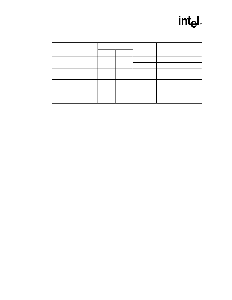
Block Lock Status(2)
Block
02h
D0 = 0
Block is unlocked
D0 = 1
Block is locked
Block Lock-Down Status(2)
Block
02h
D1 = 0
Block is not locked-down
D1 = 1
Block is locked down
Configuration Register
Partition
05h
Register Data
Protection Register Lock Status
Partition
80h
Lock Data
Protection Register
Partition
81h - 88h
Register Data
Multiple reads required to read
the entire 128-bit Protection
Register.
Notes:
1.
The address is constructed from a base address plus an offset. For example, to read the Block Lock
Status for block number 38 in a BPD, set the address to the BBA (0F8000h) plus the offset (02h),
which in this example is 0F8002h. Then examine bit 0 of the data to determine whether the block is
locked.
2.
See Section 13.1.4, “Block Lock Status” on page 75 for valid lock status.
Table 20.
Flash Device Identification Codes (Sheet 2 of 2)
Item
Address1
Data
Description
Base
Offset
相關(guān)PDF資料 |
PDF描述 |
|---|---|
| GEN12.5-120 | Programmable DC Power Supplies 750W/1500W |
| GEN12.5-60 | Programmable DC Power Supplies 750W/1500W |
| GFL750 | COPPER ALLOY, WIRE TERMINAL |
| GFL500 | COPPER ALLOY, WIRE TERMINAL |
| GFL350 | COPPER ALLOY, WIRE TERMINAL |
相關(guān)代理商/技術(shù)參數(shù) |
參數(shù)描述 |
|---|---|
| GE28F800B3BA90 | 制造商:Intel 功能描述:NOR Flash, 512K x 16, 45 Pin, Plastic, BGA |
| GE28F800B3TA90 | 制造商:INTEL 制造商全稱:Intel Corporation 功能描述:3 Volt Advanced Boot Block Flash Memory |
| GE28F800C3BA70 | 制造商:INTEL 制造商全稱:Intel Corporation 功能描述:Advanced+ Boot Block Flash Memory (C3) |
| GE28F800C3BA90 | 制造商:INTEL 制造商全稱:Intel Corporation 功能描述:Advanced+ Boot Block Flash Memory (C3) |
| GE28F800C3BC70 | 制造商:INTEL 制造商全稱:Intel Corporation 功能描述:Advanced+ Boot Block Flash Memory (C3) |
發(fā)布緊急采購(gòu),3分鐘左右您將得到回復(fù)。