- 您現(xiàn)在的位置:買賣IC網(wǎng) > PDF目錄299156 > GE28F640W30TD70 (INTEL CORP) 4M X 16 FLASH 1.8V PROM, 70 ns, PBGA56 PDF資料下載
參數(shù)資料
| 型號: | GE28F640W30TD70 |
| 廠商: | INTEL CORP |
| 元件分類: | PROM |
| 英文描述: | 4M X 16 FLASH 1.8V PROM, 70 ns, PBGA56 |
| 封裝: | 0.75 MM PITCH, VFBGA-56 |
| 文件頁數(shù): | 22/104頁 |
| 文件大小: | 1443K |
| 代理商: | GE28F640W30TD70 |
第1頁第2頁第3頁第4頁第5頁第6頁第7頁第8頁第9頁第10頁第11頁第12頁第13頁第14頁第15頁第16頁第17頁第18頁第19頁第20頁第21頁當(dāng)前第22頁第23頁第24頁第25頁第26頁第27頁第28頁第29頁第30頁第31頁第32頁第33頁第34頁第35頁第36頁第37頁第38頁第39頁第40頁第41頁第42頁第43頁第44頁第45頁第46頁第47頁第48頁第49頁第50頁第51頁第52頁第53頁第54頁第55頁第56頁第57頁第58頁第59頁第60頁第61頁第62頁第63頁第64頁第65頁第66頁第67頁第68頁第69頁第70頁第71頁第72頁第73頁第74頁第75頁第76頁第77頁第78頁第79頁第80頁第81頁第82頁第83頁第84頁第85頁第86頁第87頁第88頁第89頁第90頁第91頁第92頁第93頁第94頁第95頁第96頁第97頁第98頁第99頁第100頁第101頁第102頁第103頁第104頁
28F640W30, 28F320W30, 28F128W30
June 2005
Intel Wireless Flash Memory (W30)
Datasheet
24
Order Number: 290702, Revision: 011
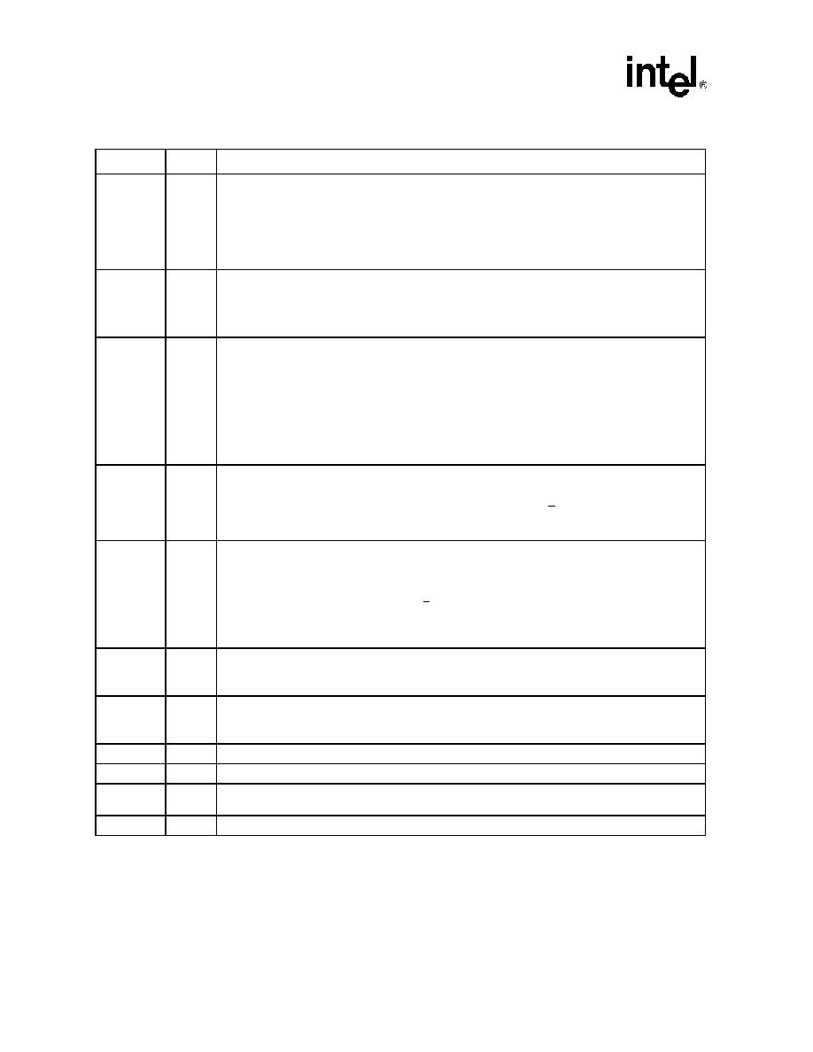
R-UB#
R-LB#
Input
RAM UPPER / LOWER BYTE ENABLES: Low-true input.
During RAM read and write cycles:
R-UB# low enables the RAM high order bytes on D[15:8].
R-LB# low enables the RAM low-order bytes on D[7:0].
R-UB# and R-LB# are available on stacked combinations with PSRAM or SRAM die, and are RFU on
flash-only stacked combinations.
F-RST#
Input
FLASH RESET: Low-true input.
F-RST# low initializes flash device internal circuitry and disables flash device operations.
F-RST# high enables flash device operation.
Exit from reset places the flash device in asynchronous read array mode.
P-Mode,
P-CRE
Input
P-Mode (PSRAM Mode): Low-true input.
P-Mode programs the Configuration Register, and enters/exits the Low Power Mode of the PSRAM
die.
P-Mode is available on stacked combinations with asynchronous-only PSRAM die.
P-CRE (PSRAM Configuration Register Enable): High-true input.
P-CRE is high, write operations load the Refresh Control Register or Bus Control Register.
P-CRE applies only on combinations with synchronous PSRAM die.
P-Mode, P-CRE is an RFU on stacked combinations without PSRAM die.
F-VPP,
F-VPEN
Power
FLASH PROGRAM AND ERASE POWER: Valid F-VPP voltage on this ball enables flash memory
device program/erase operations.
Flash memory array contents cannot be altered when F-VPP(F-VPEN) < VPPLK (VPENLK). Do not
attempt erase / program operations at invalid F-VPP (F-VPEN) voltages.
F-VPEN (Erase/Program/Block Lock Enables) is not available for L18/L30 SCSP products.
F[2:1]-VCC
Power
FLASH LOGIC POWER:
F1-VCC supplies power to the core logic of flash die #1.
F2-VCC supplies power to the core logic of flash die #2 and flash die #3.
Write operations are inhibited when F-VCC < VLKO. Do not attempt flash device operations at invalid
F-VCC voltages.
F2-VCC is available on stacked combinations with two or three flash dies, and is an RFU on stacked
combinations with only one flash die.
S-VCC
Power
SRAM POWER SUPPLY: Supplies power for SRAM operations.
S-VCC is available on stacked combinations with SRAM die, and is RFU on stacked combinations
without SRAM die.
P-VCC
Power
PSRAM POWER SUPPLY: Supplies power for PSRAM operations.
P-VCC is available on stacked combinations with PSRAM die, and is RFU on stacked combinations
without PSRAM die.
VCCQ
Power
FLASH DEVICE I/O POWER: Supply power for the flash device input and output buffers.
VSS
Power
FLASH DEVICE GROUND: Connect to system ground. Do not float any VSS connection.
RFU
—
RESERVED for FUTURE USE: Reserved for future flash device functionality/ enhancements. Contact
Intel regarding the use of balls designated RFU.
DU
—
DO NOT USE: Do not connect to any other signal, or power supply; must be left floating.
Table 6.
Signal Descriptions - QUAD+ Package (Sheet 3 of 3)
Symbol
Type
Description
相關(guān)PDF資料 |
PDF描述 |
|---|---|
| GEN12.5-120 | Programmable DC Power Supplies 750W/1500W |
| GEN12.5-60 | Programmable DC Power Supplies 750W/1500W |
| GFL750 | COPPER ALLOY, WIRE TERMINAL |
| GFL500 | COPPER ALLOY, WIRE TERMINAL |
| GFL350 | COPPER ALLOY, WIRE TERMINAL |
相關(guān)代理商/技術(shù)參數(shù) |
參數(shù)描述 |
|---|---|
| GE28F800B3BA90 | 制造商:Intel 功能描述:NOR Flash, 512K x 16, 45 Pin, Plastic, BGA |
| GE28F800B3TA90 | 制造商:INTEL 制造商全稱:Intel Corporation 功能描述:3 Volt Advanced Boot Block Flash Memory |
| GE28F800C3BA70 | 制造商:INTEL 制造商全稱:Intel Corporation 功能描述:Advanced+ Boot Block Flash Memory (C3) |
| GE28F800C3BA90 | 制造商:INTEL 制造商全稱:Intel Corporation 功能描述:Advanced+ Boot Block Flash Memory (C3) |
| GE28F800C3BC70 | 制造商:INTEL 制造商全稱:Intel Corporation 功能描述:Advanced+ Boot Block Flash Memory (C3) |
發(fā)布緊急采購,3分鐘左右您將得到回復(fù)。