- 您現(xiàn)在的位置:買賣IC網(wǎng) > PDF目錄384068 > μPD98405 (NEC Corp.) 155M ATM Integrated SAR Controller(155M ATM SAR集成控制器) PDF資料下載
參數(shù)資料
| 型號: | μPD98405 |
| 廠商: | NEC Corp. |
| 英文描述: | 155M ATM Integrated SAR Controller(155M ATM SAR集成控制器) |
| 中文描述: | 155M章綜合特區(qū)控制器自動柜員機(155M章自動柜員機特區(qū)集成控制器) |
| 文件頁數(shù): | 31/391頁 |
| 文件大?。?/td> | 3644K |
| 代理商: | ΜPD98405 |
第1頁第2頁第3頁第4頁第5頁第6頁第7頁第8頁第9頁第10頁第11頁第12頁第13頁第14頁第15頁第16頁第17頁第18頁第19頁第20頁第21頁第22頁第23頁第24頁第25頁第26頁第27頁第28頁第29頁第30頁當前第31頁第32頁第33頁第34頁第35頁第36頁第37頁第38頁第39頁第40頁第41頁第42頁第43頁第44頁第45頁第46頁第47頁第48頁第49頁第50頁第51頁第52頁第53頁第54頁第55頁第56頁第57頁第58頁第59頁第60頁第61頁第62頁第63頁第64頁第65頁第66頁第67頁第68頁第69頁第70頁第71頁第72頁第73頁第74頁第75頁第76頁第77頁第78頁第79頁第80頁第81頁第82頁第83頁第84頁第85頁第86頁第87頁第88頁第89頁第90頁第91頁第92頁第93頁第94頁第95頁第96頁第97頁第98頁第99頁第100頁第101頁第102頁第103頁第104頁第105頁第106頁第107頁第108頁第109頁第110頁第111頁第112頁第113頁第114頁第115頁第116頁第117頁第118頁第119頁第120頁第121頁第122頁第123頁第124頁第125頁第126頁第127頁第128頁第129頁第130頁第131頁第132頁第133頁第134頁第135頁第136頁第137頁第138頁第139頁第140頁第141頁第142頁第143頁第144頁第145頁第146頁第147頁第148頁第149頁第150頁第151頁第152頁第153頁第154頁第155頁第156頁第157頁第158頁第159頁第160頁第161頁第162頁第163頁第164頁第165頁第166頁第167頁第168頁第169頁第170頁第171頁第172頁第173頁第174頁第175頁第176頁第177頁第178頁第179頁第180頁第181頁第182頁第183頁第184頁第185頁第186頁第187頁第188頁第189頁第190頁第191頁第192頁第193頁第194頁第195頁第196頁第197頁第198頁第199頁第200頁第201頁第202頁第203頁第204頁第205頁第206頁第207頁第208頁第209頁第210頁第211頁第212頁第213頁第214頁第215頁第216頁第217頁第218頁第219頁第220頁第221頁第222頁第223頁第224頁第225頁第226頁第227頁第228頁第229頁第230頁第231頁第232頁第233頁第234頁第235頁第236頁第237頁第238頁第239頁第240頁第241頁第242頁第243頁第244頁第245頁第246頁第247頁第248頁第249頁第250頁第251頁第252頁第253頁第254頁第255頁第256頁第257頁第258頁第259頁第260頁第261頁第262頁第263頁第264頁第265頁第266頁第267頁第268頁第269頁第270頁第271頁第272頁第273頁第274頁第275頁第276頁第277頁第278頁第279頁第280頁第281頁第282頁第283頁第284頁第285頁第286頁第287頁第288頁第289頁第290頁第291頁第292頁第293頁第294頁第295頁第296頁第297頁第298頁第299頁第300頁第301頁第302頁第303頁第304頁第305頁第306頁第307頁第308頁第309頁第310頁第311頁第312頁第313頁第314頁第315頁第316頁第317頁第318頁第319頁第320頁第321頁第322頁第323頁第324頁第325頁第326頁第327頁第328頁第329頁第330頁第331頁第332頁第333頁第334頁第335頁第336頁第337頁第338頁第339頁第340頁第341頁第342頁第343頁第344頁第345頁第346頁第347頁第348頁第349頁第350頁第351頁第352頁第353頁第354頁第355頁第356頁第357頁第358頁第359頁第360頁第361頁第362頁第363頁第364頁第365頁第366頁第367頁第368頁第369頁第370頁第371頁第372頁第373頁第374頁第375頁第376頁第377頁第378頁第379頁第380頁第381頁第382頁第383頁第384頁第385頁第386頁第387頁第388頁第389頁第390頁第391頁
CHAPTER 2 PIN FUNCTIONS
31
(2/4)
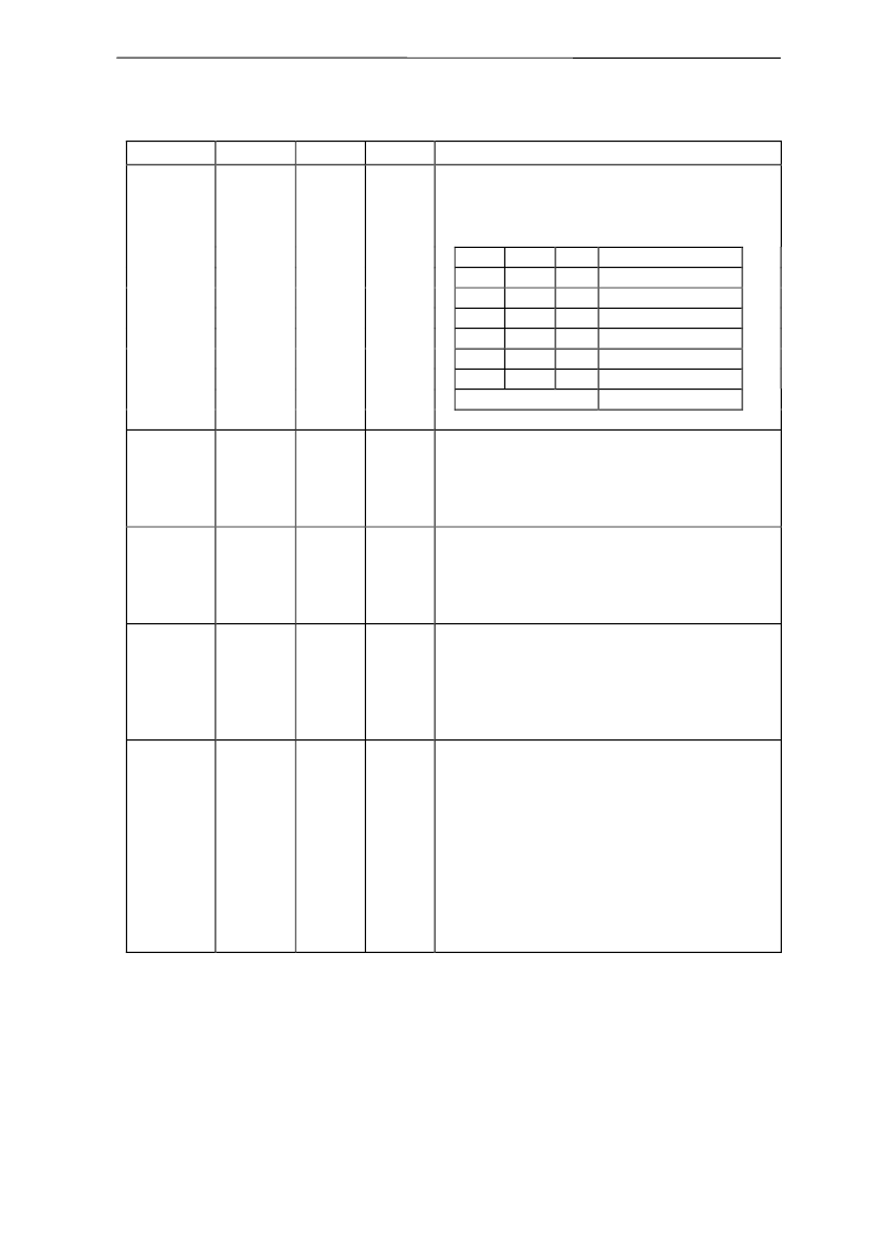
Symbol
Pin No.
I/O
I/O level
Function
SIZE2
SIZE1
SIZE0
63
64
65
O
TTL
Burst Size
The SIZE2 to SIZE0 signals indicate the size of the current
DMA transfer. These pins are provided to support interface
to buses that require an explicit burst size (e.g., S bus).
SIZE2
0
0
0
0
1
1
Others
SIZE1
0
0
1
1
0
0
SIZE0
0
1
0
1
0
1
Function
One-word transfer
Two-word burst
Four-word burst
Eight-word burst
Sixteen-word burst
Twelve-word burst
Undefined
DR/W_B
60
O
TTL
DMA Read/Write
The DR/W_B signal determines the direction of DMA
access.
1:
Read access
0:
Write access
Attention (DMA request)
The
μ
PD98405 sets the ATTN_B signal to low when
attempting to start DMA operation. Once only one word
remains to be transferred, the ATTN_B signal becomes
inactive at the rising edge of CLK.
Grant
Set the GNT_B signal to low once the bus arbiter has
granted bus mastership in response to a DMA request from
the
μ
PD98405. By detecting the GNT_B signal being set to
active low, the
μ
PD98405 assumes that bus mastership has
been granted and starts DMA operation.
Target Device Ready
RDY_B is used in DMA cycles to indicate to the
μ
PD98405
that the transaction's target device is ready to input/output
data. During the
μ
PD98405 DMA read operation, the
RDY_B signal should go low when valid data is present on
AD31 to AD0. During the
μ
PD98405 DMA write operation,
the ATTN_B signal should go low when the target device is
ready to accept data.
The timing at which the
μ
PD98405 samples the RDY_B and
ABRT_B signals can be changed to one clock earlier (early
mode) by setting an internal register (GMR).
ATTN_B
294
O
TTL
GNT_B
291
I
TTL
RDY_B
23
I
TTL
相關(guān)PDF資料 |
PDF描述 |
|---|---|
| μPD98408 | ATM Physical Interface(ATM 物理接口) |
| μPD98411 | Ultraframer DS3/E3/DS2/E2/DS1/E1/DS0 |
| μPD98501 | Network Controller(網(wǎng)絡控制器) |
| μPG103B | Wide-Band Amplifier(寬帶放大器) |
| μPG110B | 2 to 8 GHz WIDE BAND AMPLIFIER(2-8GHz 寬帶放大器) |
相關(guān)代理商/技術(shù)參數(shù) |
參數(shù)描述 |
|---|---|
| PD98CNT30QMU | 制造商:Carlo Gavazzi 功能描述:PHOTO TS PL 30M AC/DC NO+NC |
| PD9909-59 | 制造商:Philco/Philips 功能描述: |
| PD9930-51 | 制造商:Philco/Philips 功能描述: |
| PD9933-59 | 制造商:Philco/Philips 功能描述: |
| PD9941-59 | 制造商:Philco/Philips 功能描述: |
發(fā)布緊急采購,3分鐘左右您將得到回復。