- 您現(xiàn)在的位置:買賣IC網(wǎng) > PDF目錄383875 > T7234 Compliance with the New ETSI PSD Requirement PDF資料下載
參數(shù)資料
| 型號: | T7234 |
| 英文描述: | Compliance with the New ETSI PSD Requirement |
| 中文描述: | 符合新的ETSI PSD的要求 |
| 文件頁數(shù): | 44/116頁 |
| 文件大小: | 1056K |
| 代理商: | T7234 |
第1頁第2頁第3頁第4頁第5頁第6頁第7頁第8頁第9頁第10頁第11頁第12頁第13頁第14頁第15頁第16頁第17頁第18頁第19頁第20頁第21頁第22頁第23頁第24頁第25頁第26頁第27頁第28頁第29頁第30頁第31頁第32頁第33頁第34頁第35頁第36頁第37頁第38頁第39頁第40頁第41頁第42頁第43頁當(dāng)前第44頁第45頁第46頁第47頁第48頁第49頁第50頁第51頁第52頁第53頁第54頁第55頁第56頁第57頁第58頁第59頁第60頁第61頁第62頁第63頁第64頁第65頁第66頁第67頁第68頁第69頁第70頁第71頁第72頁第73頁第74頁第75頁第76頁第77頁第78頁第79頁第80頁第81頁第82頁第83頁第84頁第85頁第86頁第87頁第88頁第89頁第90頁第91頁第92頁第93頁第94頁第95頁第96頁第97頁第98頁第99頁第100頁第101頁第102頁第103頁第104頁第105頁第106頁第107頁第108頁第109頁第110頁第111頁第112頁第113頁第114頁第115頁第116頁
Data Sheet
January 1998
T7256 Single-Chip NT1 (SCNT1) Transceiver
40
Lucent Technologies Inc.
Microprocessor Interface Description
(continued)
Timing
(continued)
Note: If SCLK is initially low, it must be held high for >300
μ
s before its first falling edge. From that point forward, the above timing applies.
5-2302 (C)
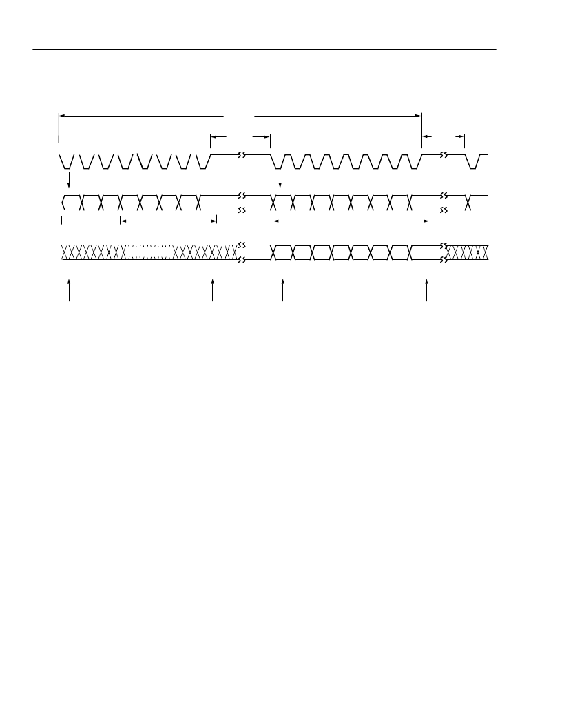
Figure 14. Synchronous Microprocessor Port Interface Format
SCLK
SDI
SDO
1
2
3
4
5
6
7
8
CA7
CA6
CA5
CA4
CA3
CA2
CA1
CA0
COMMAND
MSB
LSB
MSB
LSB
SHIFT IN
SAMPLE SHIFT IN
1
2
3
4
5
6
7
8
DI7
DI6
DI5
DI4
DI3
DI2
DI0
DI1
DO7
DO6
DO5
DO4
DO3
DO2
DO0
DO1
DON'T CARE
≤
300 μs
1
CA7
≥
10 μs
≥
10 μs
ADDRESS
DATA SHIFT OUT
Figure 14 shows the basic transfer format. All data
transfers are initiated by the microprocessor, although
the interrupt may indicate to the microprocessor that a
register read or write is required. The microprocessor
should normally hold the SCK pin high during inactive
periods and only make transitions during register trans-
fers. The maximum clock rate of SCK is 960 kHz. Data
changes on the falling edge of SCK and is latched on
the rising edge of SCK.
Each complete serial transfer consists of 2 bytes
(8 bits/byte). The first byte of data received over the
SDI pin from the microprocessor consists of
command/address information that includes a 5-bit reg-
ister address in the least significant bit positions
(CA4—CA0) and a 3-bit command field in the most sig-
nificant bit positions (CA7—CA5). The byte is defined
as follows:
I
Bits CA7—CA5: 001 = read, 010 = write, all other bit
patterns will be ignored.
I
Bits CA4—CA0: 00000 = register address 0,
00001 = register address 1, etc.
The second byte of data received over the SDI pin con-
sists of write data for CA7—CA5 = 010 (write) or don't
care information for CA7—CA5 = 001 (read).
The data transmitted over the SDO pin to the micropro-
cessor during the first byte transfer is a don't care for
both read and write operations. The second byte trans-
mitted over the SDO pin consists of read data for CA7—
CA5 = 001 (read) or don't care information for CA7—
CA5 = 010 (write).
In order for the T7256 to recognize the identity (com-
mand/address or data) of the byte being received, it is
required that the time allowed to transfer an entire
instruction (time from the receipt of the first bit of the
command/address byte to the last bit of the data byte)
be limited to less than 300
μ
s. This limits the minimum
SCK rate to 60 kHz. If the complete instruction is
received in less than 300
μ
s, the T7256 accepts the
instruction immediately and is ready to receive the next
instruction after a 10
μ
s delay. If the complete instruc-
tion is not received within 300
μ
s, the bits received in
the previous 300
μ
s are discarded and the interface is
prepared to receive a new instruction after a 10
μ
s
delay. In addition, a minimum 10
μ
s delay must exist
between the command/address and data bytes.
相關(guān)PDF資料 |
PDF描述 |
|---|---|
| T7234A | Compliance with the New ETSI PSD Requirement |
| T7237A | Compliance with the New ETSI PSD Requirement |
| T7256A | Compliance with the New ETSI PSD Requirement |
| T7288 | CEPT/E1 Line Interface(CEPT/E1 線接口) |
| T7290A | DS1/T1/CEPT/E1 Line Interface(DS1/T1/CEPT/E1 線接口) |
相關(guān)代理商/技術(shù)參數(shù) |
參數(shù)描述 |
|---|---|
| T7234A | 制造商:AGERE 制造商全稱:AGERE 功能描述:Compliance with the New ETSI PSD Requirement |
| T7237 | 制造商:未知廠家 制造商全稱:未知廠家 功能描述:Compliance with the New ETSI PSD Requirement |
| T7237A | 制造商:AGERE 制造商全稱:AGERE 功能描述:Compliance with the New ETSI PSD Requirement |
| T7240 | 制造商:TE Connectivity 功能描述: |
| T7-241A5 | 功能描述:撥動開關(guān) ON NONE OFF 2 Pole Standard Bat Handle RoHS:否 制造商:OTTO 觸點形式: 開關(guān)功能: 電流額定值: 電壓額定值 AC: 電壓額定值 DC: 功率額定值: 端接類型: 安裝風(fēng)格: 端子密封: 觸點電鍍: 照明: |
發(fā)布緊急采購,3分鐘左右您將得到回復(fù)。