- 您現(xiàn)在的位置:買賣IC網(wǎng) > PDF目錄384024 > TMX320DM6446ZWT (Texas Instruments, Inc.) Digital Media System on-Chip PDF資料下載
參數(shù)資料
| 型號(hào): | TMX320DM6446ZWT |
| 廠商: | Texas Instruments, Inc. |
| 英文描述: | Digital Media System on-Chip |
| 中文描述: | 數(shù)字媒體系統(tǒng)芯片 |
| 文件頁數(shù): | 30/214頁 |
| 文件大小: | 1699K |
| 代理商: | TMX320DM6446ZWT |
第1頁第2頁第3頁第4頁第5頁第6頁第7頁第8頁第9頁第10頁第11頁第12頁第13頁第14頁第15頁第16頁第17頁第18頁第19頁第20頁第21頁第22頁第23頁第24頁第25頁第26頁第27頁第28頁第29頁當(dāng)前第30頁第31頁第32頁第33頁第34頁第35頁第36頁第37頁第38頁第39頁第40頁第41頁第42頁第43頁第44頁第45頁第46頁第47頁第48頁第49頁第50頁第51頁第52頁第53頁第54頁第55頁第56頁第57頁第58頁第59頁第60頁第61頁第62頁第63頁第64頁第65頁第66頁第67頁第68頁第69頁第70頁第71頁第72頁第73頁第74頁第75頁第76頁第77頁第78頁第79頁第80頁第81頁第82頁第83頁第84頁第85頁第86頁第87頁第88頁第89頁第90頁第91頁第92頁第93頁第94頁第95頁第96頁第97頁第98頁第99頁第100頁第101頁第102頁第103頁第104頁第105頁第106頁第107頁第108頁第109頁第110頁第111頁第112頁第113頁第114頁第115頁第116頁第117頁第118頁第119頁第120頁第121頁第122頁第123頁第124頁第125頁第126頁第127頁第128頁第129頁第130頁第131頁第132頁第133頁第134頁第135頁第136頁第137頁第138頁第139頁第140頁第141頁第142頁第143頁第144頁第145頁第146頁第147頁第148頁第149頁第150頁第151頁第152頁第153頁第154頁第155頁第156頁第157頁第158頁第159頁第160頁第161頁第162頁第163頁第164頁第165頁第166頁第167頁第168頁第169頁第170頁第171頁第172頁第173頁第174頁第175頁第176頁第177頁第178頁第179頁第180頁第181頁第182頁第183頁第184頁第185頁第186頁第187頁第188頁第189頁第190頁第191頁第192頁第193頁第194頁第195頁第196頁第197頁第198頁第199頁第200頁第201頁第202頁第203頁第204頁第205頁第206頁第207頁第208頁第209頁第210頁第211頁第212頁第213頁第214頁
www.ti.com
P
TMS320DM6446
Digital Media System on-Chip
SPRS283–DECEMBER 2005
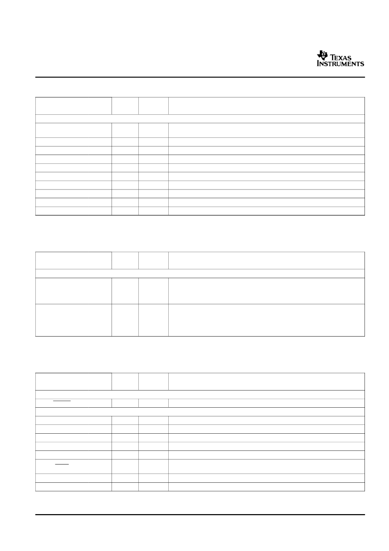
Table 2-10. Oscillator/PLL Terminal Functions
SIGNAL
NAME
IPD/
IPU
(2)
TYPE
(1)
DESCRIPTION
NO.
OSCILLATOR, PLL
Crystal input MXI for MX oscillator (system oscillator, typically 27 MHz).
If the internal oscillator is bypassed, this is the external oscillator clock input.
Crystal output for MX oscillator
1.8V power supply for MX oscillator
Ground for MX oscillator
Crystal input for M24 oscillator (24 MHz for USB)
Crystal output for M24 oscillator
1.8V power supply for M24 oscillator
Ground for M24 oscillator
1.8 Volt power supply for PLLs (system and USB)
Core voltage reference for PLL logic and bandgap backup
MXI/
CLKIN
MXO
MXV
DD
MXV
SS
M24XI
M24XO
M24V
DD
M24V
SS
PLLV
DD18
APLLREFV
L1
I
M1
L5
L2
F18
F19
F16
F17
M2
M3
O
S
GND
I
O
S
GND
S
S
(1)
(2)
I = Input, O = Output, Z = High impedance, S = Supply voltage, GND = Ground, A = Analog signal
IPD = Internal pulldown, IPU = Internal pullup. (To pull up a signal to the opposite supply rail, a 1-k
resistor should be used.)
Table 2-11. Clock Generator Terminal Functions
SIGNAL
NAME
IPD/
IPU
(2)
TYPE
(1)
DESCRIPTION
NO.
CLOCK GENERATOR
This pin is multiplexed between the PLL1 clock generator and GPIO. For the PLL1
clock generator, it is clock output CLK_OUT0. This is configurable for 13.5 MHz or
27 MHz clock outputs.
For GPIO, it is GPIO48 [default].
This pin is multiplexed between the USB clock generator, timer, and GPIO. For
the USB clock generator, it is clock output CLK_OUT1. This is configurable for 12
MHz or 24 MHz clock outputs.
For Timer0, it is the timer event capture input TIM_IN.
For GPIO, it is GPIO49 [default].
CLK_OUT0/
GPIO48
K1
I/O/Z
IPD
CLK_OUT1/
TIM_IN/
GPIO49
E19
I/O/Z
IPD
(1)
(2)
I = Input, O = Output, Z = High impedance, S = Supply voltage, GND = Ground, A = Analog signal
IPD = Internal pulldown, IPU = Internal pullup. (To pull up a signal to the opposite supply rail, a 1-k
resistor should be used.)
Table 2-12. RESET and JTAG Terminal Functions
SIGNAL
NAME
IPD/
IPU
(2)
TYPE
(1)
DESCRIPTION
NO.
RESET
RESET
L4
I
IPU
This is the active low Global reset input.
JTAG
TMS
TDO
TDI
TCK
RTCK
E6
B5
A5
A6
B6
I
IPU
JTAG test-port mode select input
JTAG test-port data output
JTAG test-port data input
JTAG test-port clock input
JTAG test-port return clock output
O/Z
I
I
O/Z
IPU
IPU
JTAG test-port reset. For IEEE 1149.1 JTAG compatibility, see the IEEE 1149.1
JTAG compatibility statement portion of this data sheet.
Emulation pin 1
Emulation pin 0
TRST
D7
I
IPD
EMU1
EMU0
C6
D6
I/O/Z
I/O/Z
IPU
IPU
(1)
(2)
I = Input, O = Output, Z = High impedance, S = Supply voltage, GND = Ground, A = Analog signal
IPD = Internal pulldown, IPU = Internal pullup. (To pull up a signal to the opposite supply rail, a 1-k
resistor should be used.)
Device Overview
30
相關(guān)PDF資料 |
PDF描述 |
|---|---|
| TN28F010-90 | 28F010 1024K (128K X 8) CMOS FLASH MEMORY |
| TN28F010-120 | 28F010 1024K (128K X 8) CMOS FLASH MEMORY |
| TN28F010-150 | 28F010 1024K (128K X 8) CMOS FLASH MEMORY |
| TN28F020-90 | 28F020 2048K (256K X 8) CMOS FLASH MEMORY |
| TN28F020-150 | 28F020 2048K (256K X 8) CMOS FLASH MEMORY |
相關(guān)代理商/技術(shù)參數(shù) |
參數(shù)描述 |
|---|---|
| TMX320DM6467TZUT1 | 制造商:Texas Instruments 功能描述: |
| TMX320DM6467ZUT | 功能描述:數(shù)字信號(hào)處理器和控制器 - DSP, DSC Dig Media System-on- Chip RoHS:否 制造商:Microchip Technology 核心:dsPIC 數(shù)據(jù)總線寬度:16 bit 程序存儲(chǔ)器大小:16 KB 數(shù)據(jù) RAM 大小:2 KB 最大時(shí)鐘頻率:40 MHz 可編程輸入/輸出端數(shù)量:35 定時(shí)器數(shù)量:3 設(shè)備每秒兆指令數(shù):50 MIPs 工作電源電壓:3.3 V 最大工作溫度:+ 85 C 封裝 / 箱體:TQFP-44 安裝風(fēng)格:SMD/SMT |
| TMX320DM647ZUT720 | 制造商:TI 制造商全稱:Texas Instruments 功能描述:Digital Media Processor |
| TMX320DM647ZUT900 | 制造商:TI 制造商全稱:Texas Instruments 功能描述:Digital Media Processor |
| TMX320DM648ACUT7 | 制造商:Texas Instruments 功能描述:- Trays |
發(fā)布緊急采購,3分鐘左右您將得到回復(fù)。