- 您現(xiàn)在的位置:買賣IC網(wǎng) > PDF目錄384024 > TMX320DM6446ZWT (Texas Instruments, Inc.) Digital Media System on-Chip PDF資料下載
參數(shù)資料
| 型號(hào): | TMX320DM6446ZWT |
| 廠商: | Texas Instruments, Inc. |
| 英文描述: | Digital Media System on-Chip |
| 中文描述: | 數(shù)字媒體系統(tǒng)芯片 |
| 文件頁數(shù): | 106/214頁 |
| 文件大?。?/td> | 1699K |
| 代理商: | TMX320DM6446ZWT |
第1頁第2頁第3頁第4頁第5頁第6頁第7頁第8頁第9頁第10頁第11頁第12頁第13頁第14頁第15頁第16頁第17頁第18頁第19頁第20頁第21頁第22頁第23頁第24頁第25頁第26頁第27頁第28頁第29頁第30頁第31頁第32頁第33頁第34頁第35頁第36頁第37頁第38頁第39頁第40頁第41頁第42頁第43頁第44頁第45頁第46頁第47頁第48頁第49頁第50頁第51頁第52頁第53頁第54頁第55頁第56頁第57頁第58頁第59頁第60頁第61頁第62頁第63頁第64頁第65頁第66頁第67頁第68頁第69頁第70頁第71頁第72頁第73頁第74頁第75頁第76頁第77頁第78頁第79頁第80頁第81頁第82頁第83頁第84頁第85頁第86頁第87頁第88頁第89頁第90頁第91頁第92頁第93頁第94頁第95頁第96頁第97頁第98頁第99頁第100頁第101頁第102頁第103頁第104頁第105頁當(dāng)前第106頁第107頁第108頁第109頁第110頁第111頁第112頁第113頁第114頁第115頁第116頁第117頁第118頁第119頁第120頁第121頁第122頁第123頁第124頁第125頁第126頁第127頁第128頁第129頁第130頁第131頁第132頁第133頁第134頁第135頁第136頁第137頁第138頁第139頁第140頁第141頁第142頁第143頁第144頁第145頁第146頁第147頁第148頁第149頁第150頁第151頁第152頁第153頁第154頁第155頁第156頁第157頁第158頁第159頁第160頁第161頁第162頁第163頁第164頁第165頁第166頁第167頁第168頁第169頁第170頁第171頁第172頁第173頁第174頁第175頁第176頁第177頁第178頁第179頁第180頁第181頁第182頁第183頁第184頁第185頁第186頁第187頁第188頁第189頁第190頁第191頁第192頁第193頁第194頁第195頁第196頁第197頁第198頁第199頁第200頁第201頁第202頁第203頁第204頁第205頁第206頁第207頁第208頁第209頁第210頁第211頁第212頁第213頁第214頁
www.ti.com
P
5.7.2
DSP Interrupts
TMS320DM6446
Digital Media System on-Chip
SPRS283–DECEMBER 2005
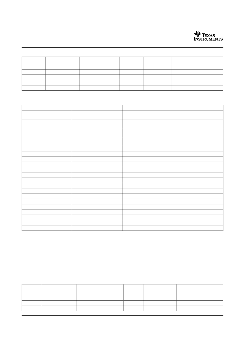
Table 5-16. DM6446 MPU Interrupts (continued)
MPU
MPU
INTERRUPT
NUMBER
28
29
30
31
ACRONYM
SOURCE
INTERRUPT
NUMBER
60
61
62
63
ACRONYM
SOURCE
-
DDRINT
EMIFAINT
VLQINT
Reserved
DDR2 Memory Controller
EMIFA
VLYNQ
GPIOBNK4
COMMTX
COMMRX
EMUINT
GPIO Bank 4
ARMSS
ARMSS
E2ICE
Table 5-17. ARM Interrupt Controller Registers
HEX ADDRESS
ACRONYM
REGISTER DESCRIPTION
0x01C4 8000
FIQ Interrupt Status 0 [Interrupt Status of INT[31:0] (If Mapped to
FIQ)]
FIQ Interrupt Status 1 [Interrupt Status of INT[63:32] (If Mapped to
FIQ)]
IRQ Interrupt Status 0 [Interrupt Status of INT[31:0] (If Mapped to
IRQ)]
IRQ Interrupt Status 1 [Interrupt Status of INT[63:32] (If Mapped to
IRQ)]
Entry Address [28:0] for Valid FIQ Interrupt
Entry Address [28:0] for Valid IRQ Interrupt
Interrupt Enable Register 0
Interrupt Enable Register 1
Interrupt Operation Control Register
Interrupt Entry Table Base Address Register
Reserved
Interrupt 0-7 Priority Select
Interrupt 8-15 Priority Select
Interrupt 16-23 Priority Select
Interrupt 24-31 Priority Select
Interrupt 32-39 Priority Select
Interrupt 40-47 Priority Select
Interrupt 48-55 Priority Select
Interrupt 56-63 Priority Select
Reserved
FIQ0
0x01C4 8004
FIQ1
0x01C4 8008
IRQ0
0x01C4 800C
IRQ1
0x01C4 8010
0x01C4 8014
0x01C4 8018
0x01C4 801C
0x01C4 8020
0x01C4 8024
0x01C4 8028 - 0x01C4 802F
0x01C4 8030
0x01C4 8034
0x01C4 8038
0x01C4 803C
0x01C4 8040
0x01C4 8044
0x01C4 8048
0x01C4 804C
0x01C4 8050 - 0x01C4 83FF
FIQENTRY
IRQENTRY
EINT0
EINT1
INCTL
EABASE
-
INTPRI0
INTPRI1
INTPRI2
INTPRI3
INTPRI4
INTPRI5
INTPRI6
INTPRI7
-
The C64x+ DSP interrupt controller combines device events into 12 prioritized interrupts. The source for
each of the 12 CPU interrupts is user programmable and is listed in
Table 5-18
. Also, the interrupt
controller controls the generation of the CPU exception, NMI, and emulation interrupts and the generation
of AEG events.
Table 5-19
summarizes the C64x+ interrupt controller registers and memory locations. For
more details on DSP interrupt control, see the
Documentation Support
section for the DSP Subsystem
User's Guide.
Table 5-18. DM6446 DSP Interrupts
DSP
DSP
INTERRUP
T
NUMBER
0
1
INTERRUP
T
NUMBER
64
65
ACRONYM
SOURCE
ACRONYM
SOURCE
EVT0
EVT1
C64x+ Int Ctl 0
C64x+ Int Ctl 1
Reserved
Reserved
106
Peripheral and Electrical Specifications
相關(guān)PDF資料 |
PDF描述 |
|---|---|
| TN28F010-90 | 28F010 1024K (128K X 8) CMOS FLASH MEMORY |
| TN28F010-120 | 28F010 1024K (128K X 8) CMOS FLASH MEMORY |
| TN28F010-150 | 28F010 1024K (128K X 8) CMOS FLASH MEMORY |
| TN28F020-90 | 28F020 2048K (256K X 8) CMOS FLASH MEMORY |
| TN28F020-150 | 28F020 2048K (256K X 8) CMOS FLASH MEMORY |
相關(guān)代理商/技術(shù)參數(shù) |
參數(shù)描述 |
|---|---|
| TMX320DM6467TZUT1 | 制造商:Texas Instruments 功能描述: |
| TMX320DM6467ZUT | 功能描述:數(shù)字信號(hào)處理器和控制器 - DSP, DSC Dig Media System-on- Chip RoHS:否 制造商:Microchip Technology 核心:dsPIC 數(shù)據(jù)總線寬度:16 bit 程序存儲(chǔ)器大小:16 KB 數(shù)據(jù) RAM 大小:2 KB 最大時(shí)鐘頻率:40 MHz 可編程輸入/輸出端數(shù)量:35 定時(shí)器數(shù)量:3 設(shè)備每秒兆指令數(shù):50 MIPs 工作電源電壓:3.3 V 最大工作溫度:+ 85 C 封裝 / 箱體:TQFP-44 安裝風(fēng)格:SMD/SMT |
| TMX320DM647ZUT720 | 制造商:TI 制造商全稱:Texas Instruments 功能描述:Digital Media Processor |
| TMX320DM647ZUT900 | 制造商:TI 制造商全稱:Texas Instruments 功能描述:Digital Media Processor |
| TMX320DM648ACUT7 | 制造商:Texas Instruments 功能描述:- Trays |
發(fā)布緊急采購,3分鐘左右您將得到回復(fù)。