- 您現(xiàn)在的位置:買賣IC網(wǎng) > PDF目錄370261 > FW82439TX Controller Miscellaneous - Datasheet Reference PDF資料下載
參數(shù)資料
| 型號: | FW82439TX |
| 英文描述: | Controller Miscellaneous - Datasheet Reference |
| 中文描述: | 控制器雜項-數(shù)據(jù)表參考 |
| 文件頁數(shù): | 69/102頁 |
| 文件大小: | 759K |
| 代理商: | FW82439TX |
第1頁第2頁第3頁第4頁第5頁第6頁第7頁第8頁第9頁第10頁第11頁第12頁第13頁第14頁第15頁第16頁第17頁第18頁第19頁第20頁第21頁第22頁第23頁第24頁第25頁第26頁第27頁第28頁第29頁第30頁第31頁第32頁第33頁第34頁第35頁第36頁第37頁第38頁第39頁第40頁第41頁第42頁第43頁第44頁第45頁第46頁第47頁第48頁第49頁第50頁第51頁第52頁第53頁第54頁第55頁第56頁第57頁第58頁第59頁第60頁第61頁第62頁第63頁第64頁第65頁第66頁第67頁第68頁當前第69頁第70頁第71頁第72頁第73頁第74頁第75頁第76頁第77頁第78頁第79頁第80頁第81頁第82頁第83頁第84頁第85頁第86頁第87頁第88頁第89頁第90頁第91頁第92頁第93頁第94頁第95頁第96頁第97頁第98頁第99頁第100頁第101頁第102頁
Extended Temperature 82439TX (MTXC) Datasheet
69
PRELIMINARY
synchronized to the PCI clock. To not reset the suspend well within the MTXC, the PIIX4 will drive the
SUS_STAT# signal just after the SUSCLK signal has gone high. To reset the resume well within the MTXC,
the PIIX4 will drive the SUS_STAT# signal while the SUSCLK is disabled (low). Because of this functionality,
SUSCLK should not be inverted for any reason in applications.
4.7.
PCI Interface
The MTXC integrates a high performance interface to the PCI local bus taking full advantage of the high
bandwidth and low latency of PCI. The MTXC is fully PCI 2.1 compliant. Table 22 lists the PCI bus
commands supported. Five PCI masters are supported by the integrated arbiter including the PIIX4 and four
general PCI masters. The MTXC acts as a PCI master for CPU accesses to PCI. The PCI bus is clocked at
one half the frequency of the CPU clock. This divided synchronous interface minimizes latency for CPU-to-
PCI cycles and PCI-to-main memory cycles.
The MTXC integrates posted write buffers for CPU memory writes to PCI. Back-to-back sequential memory
writes to PCI are converted to burst writes on PCI. This feature allows the CPU to continue posting DWord
writes at the maximum bandwidth for the Pentium processor for the highest possible transfer rates to the
graphics frame buffer.
Read prefetch and write posting buffers in the MTXC enable PCI masters to access main memory at up to
120 MB/sec. The MTXC incorporates a snoop ahead feature that allows PCI masters to continue bursting on
both reads and writes even as the bursts cross cache line boundaries.
The MTXC forwards each of the CPU shutdown, Halt, and Stop Grant cycles to the PCI bus as special
cycles. These cycles are terminated on PCI as master abort and a BRDY# is returned to the CPU. The Stop
Grant cycle is propagated with 0002h in the message field and 0012h in the message dependent data field.
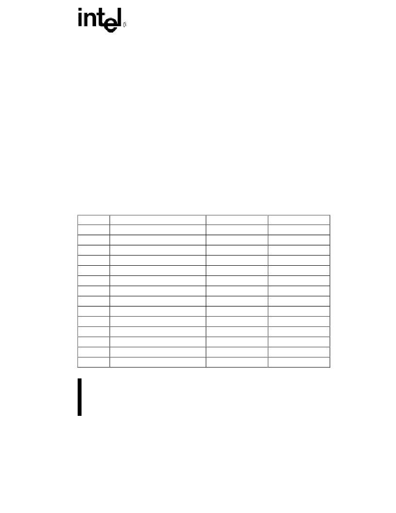
Table 22. PCI Commands
C/BE#
Command
Target Support
Initiator Support
0000
Interrupt Acknowledge
NO
YES
0001
Special cycle
NO
YES
0010
I/O read
YES
YES
0011
I/O write
YES
YES
0100
reserved
NO
NO
0101
reserved
NO
NO
0110
Memory read
YES
YES
0111
Memory write
YES
YES
1000
reserved
NO
NO
1001
reserved
NO
NO
1010
Configuration Read
NO
YES
1011
Configuration Write
NO
YES
1100
Memory Read Multiple
As Memory Read
NO
1101
Dual Address Cycle
NO
NO
相關(guān)PDF資料 |
PDF描述 |
|---|---|
| FW82815 | Controller Miscellaneous - Datasheet Reference |
| FWA-25A10F | Fuse |
| FWA-30A10F | Fuse |
| FWA-35A21F | Fuse |
| FWA-40A21F | Fuse |
相關(guān)代理商/技術(shù)參數(shù) |
參數(shù)描述 |
|---|---|
| FW82439TX S L28T | 制造商:Intel 功能描述:System Controller 324-Pin BGA |
| FW82439TX S L3BT | 制造商:Intel 功能描述:System Controller |
| FW82439TX S L28T | 制造商:Intel 功能描述: |
| FW82439TX S L3BT | 制造商:Intel 功能描述:System Controller |
| FW82439TXSL28T | 功能描述:IC 82439TX SYS CTRL MTXC 324BGA RoHS:否 類別:集成電路 (IC) >> 接口 - 控制器 系列:- 標準包裝:4,900 系列:- 控制器類型:USB 2.0 控制器 接口:串行 電源電壓:3 V ~ 3.6 V 電流 - 電源:135mA 工作溫度:0°C ~ 70°C 安裝類型:表面貼裝 封裝/外殼:36-VFQFN 裸露焊盤 供應(yīng)商設(shè)備封裝:36-QFN(6x6) 包裝:* 其它名稱:Q6396337A |
發(fā)布緊急采購,3分鐘左右您將得到回復(fù)。