- 您現(xiàn)在的位置:買賣IC網(wǎng) > PDF目錄384032 > TVP3026-220 (Texas Instruments, Inc.) Video Interface PALETTE Exract(組合像素模式視頻接口調(diào)色器) PDF資料下載
參數(shù)資料
| 型號(hào): | TVP3026-220 |
| 廠商: | Texas Instruments, Inc. |
| 英文描述: | Video Interface PALETTE Exract(組合像素模式視頻接口調(diào)色器) |
| 中文描述: | 視頻接口調(diào)色板Exract(組合像素模式視頻接口調(diào)色器) |
| 文件頁數(shù): | 52/107頁 |
| 文件大?。?/td> | 707K |
| 代理商: | TVP3026-220 |
第1頁第2頁第3頁第4頁第5頁第6頁第7頁第8頁第9頁第10頁第11頁第12頁第13頁第14頁第15頁第16頁第17頁第18頁第19頁第20頁第21頁第22頁第23頁第24頁第25頁第26頁第27頁第28頁第29頁第30頁第31頁第32頁第33頁第34頁第35頁第36頁第37頁第38頁第39頁第40頁第41頁第42頁第43頁第44頁第45頁第46頁第47頁第48頁第49頁第50頁第51頁當(dāng)前第52頁第53頁第54頁第55頁第56頁第57頁第58頁第59頁第60頁第61頁第62頁第63頁第64頁第65頁第66頁第67頁第68頁第69頁第70頁第71頁第72頁第73頁第74頁第75頁第76頁第77頁第78頁第79頁第80頁第81頁第82頁第83頁第84頁第85頁第86頁第87頁第88頁第89頁第90頁第91頁第92頁第93頁第94頁第95頁第96頁第97頁第98頁第99頁第100頁第101頁第102頁第103頁第104頁第105頁第106頁第107頁
2–38
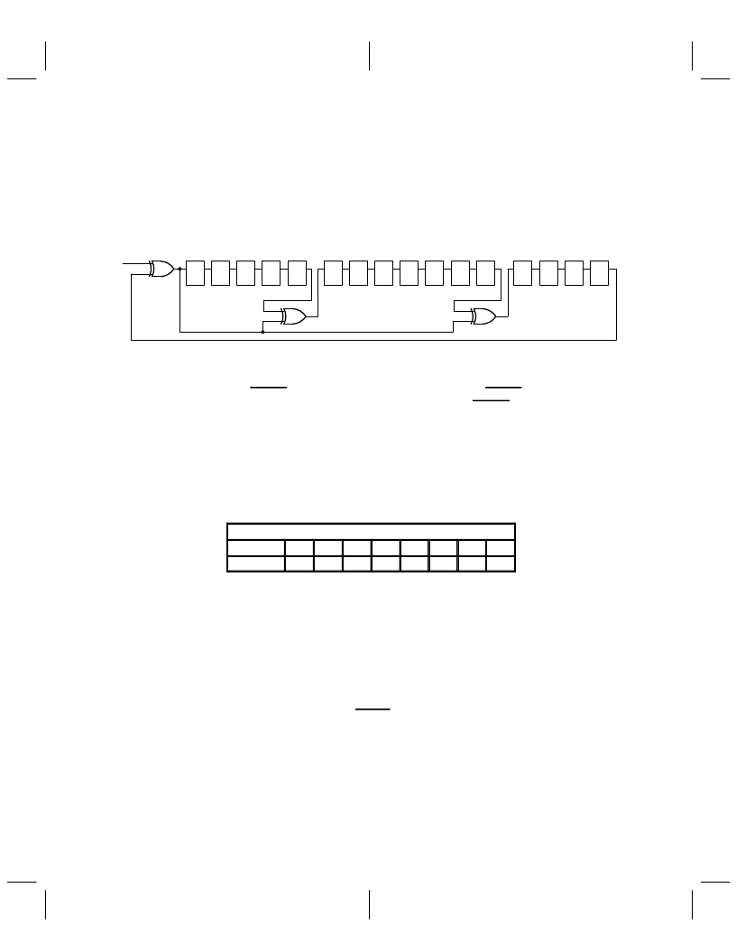
the 24 different DAC data inputs. The 16-bit remainder that is calculated on the individual DAC data line can
be read from the CRC remainder LSB and CRC remainder MSB registers. See subsection 2.15.9, CRC
Remainder LSB and MSB Registers and subsection 2.15.10, CRC Bit-Select Register for the CRC register
bit definitions.
As long as the display pattern for each screen remains fixed, the CRC result should remain constant. When
the CRC result changes, an error condition should be assumed. The CRC is calculated using the algorithm
depicted by the circuit in Figure 2–11. The user can calculate and store the CRC remainder for a test screen
in software and compare this to the TVP3026 calculated CRC remainder to verify data integrity.
LSB
D Q
15
D Q
14
D Q
13
DQ
12
DQ
11
DQ
10
DQ
9
DQ
8
DQ
7
DQ
6
DQ
5
DQ
4
DQ
3
D Q
2
D Q
1
DQ
0
DATAIN
Q0
MSB
Figure 2–11. CRC Algorithm
2.11.2
Sense Comparator Output and Test Register
The TVP3026 provides a SENSE output to support system diagnostics. SENSE can determine the
presence of the CRT monitor or verify that the RGB termination is correct. SENSE is reset to 0 when one
or more of the DAC outputs exceeds the internal comparator voltage of 350 mV. The internal 350-mV
reference has a tolerance of
±
50 mV when using an external 1.235-V reference. When the internal voltage
reference is used, the tolerance is higher.
The sense comparators are also integrated with the sense test register (index: 0x3A) so that the comparison
results for the red, green, and blue comparators can be read independently through the 8-bit microinterface.
When the sense test register (STR) is read, the results are indicated in the bit positions of Table 2-24.
Table 2–24. Sense Test Register Results
INDEX: 0x3A, ACCESS: R/W, DEFAULT: UNINITIALIZED
STR BITS
D7
D6
D5
D4
D3
D2
D1
D0
Data
DIS
0
0
0
0
R
G
B
where: R = set to 1 if IOR > 350 mV
G = set to 1 if IOG > 350 mV
B = set to 1 if IOB > 350 mV
D6 – D3 are reserved
D7 is disable (set to 1) bit
NOTE
D7 can be set to 1 to disable the sense comparison function. At reset, the sense
comparison is enabled (D7 = 0). D6–D3 are reserved. When this register is written
to, to disable the sense comparator function, bits D6–D0 need to be reset 0.
Both the SENSE output and the sense test register are latched by the falling edge
of the internally sampled blank signal (SYSBL or VGABL depending on bit MCR6).
In order to have stable voltage inputs to the comparators, the frame-buffer inputs
should be set such that data entering the DACs remains unchanged for a sufficient
period of time prior to and after the BLANK signal falling edge.
Identification Code
An ID register with a hardwired code is provided that can be used as a software identification of the device
for different versions of the system design. The ID register is read only through index 0x3F. The value defined
for the TVP3026 is 0x26.
2.11.3
相關(guān)PDF資料 |
PDF描述 |
|---|---|
| TVP3026-250 | Video Interface PALETTE Exract(組合像素模式視頻接口調(diào)色器) |
| TX24 | 60.8 MM 5 X 8 DOT MATRIX DISPLAYS |
| TXB0102DCTR | 2-BIT BIDIRECTIONAL VOLTAGE-LEVEL TRANSLATOR WITH AUTO DIRECTION SENSING AND 【15-kV ESD PROTECTION |
| TXB0102DCTT | 2-BIT BIDIRECTIONAL VOLTAGE-LEVEL TRANSLATOR WITH AUTO DIRECTION SENSING AND 【15-kV ESD PROTECTION |
| TZX7V5D | surface mount silicon Zener diodes |
相關(guān)代理商/技術(shù)參數(shù) |
參數(shù)描述 |
|---|---|
| TVP3026-220AMDN | 制造商:TI 制造商全稱:Texas Instruments 功能描述:Video Interface Palette |
| TVP3026-220APCE | 制造商:TI 制造商全稱:Texas Instruments 功能描述:Video Interface Palette |
| TVP3026-220BMDN | 制造商:TI 制造商全稱:Texas Instruments 功能描述:Video Interface Palette |
| TVP3026-220BPCE | 制造商:Rochester Electronics LLC 功能描述:- Bulk |
| TVP3026-220MDN | 制造商:未知廠家 制造商全稱:未知廠家 功能描述:Video DAC with Color Palette (RAMDAC) |
發(fā)布緊急采購,3分鐘左右您將得到回復(fù)。