- 您現(xiàn)在的位置:買賣IC網(wǎng) > PDF目錄384032 > TVP3026-220 (Texas Instruments, Inc.) Video Interface PALETTE Exract(組合像素模式視頻接口調(diào)色器) PDF資料下載
參數(shù)資料
| 型號(hào): | TVP3026-220 |
| 廠商: | Texas Instruments, Inc. |
| 英文描述: | Video Interface PALETTE Exract(組合像素模式視頻接口調(diào)色器) |
| 中文描述: | 視頻接口調(diào)色板Exract(組合像素模式視頻接口調(diào)色器) |
| 文件頁(yè)數(shù): | 26/107頁(yè) |
| 文件大小: | 707K |
| 代理商: | TVP3026-220 |
第1頁(yè)第2頁(yè)第3頁(yè)第4頁(yè)第5頁(yè)第6頁(yè)第7頁(yè)第8頁(yè)第9頁(yè)第10頁(yè)第11頁(yè)第12頁(yè)第13頁(yè)第14頁(yè)第15頁(yè)第16頁(yè)第17頁(yè)第18頁(yè)第19頁(yè)第20頁(yè)第21頁(yè)第22頁(yè)第23頁(yè)第24頁(yè)第25頁(yè)當(dāng)前第26頁(yè)第27頁(yè)第28頁(yè)第29頁(yè)第30頁(yè)第31頁(yè)第32頁(yè)第33頁(yè)第34頁(yè)第35頁(yè)第36頁(yè)第37頁(yè)第38頁(yè)第39頁(yè)第40頁(yè)第41頁(yè)第42頁(yè)第43頁(yè)第44頁(yè)第45頁(yè)第46頁(yè)第47頁(yè)第48頁(yè)第49頁(yè)第50頁(yè)第51頁(yè)第52頁(yè)第53頁(yè)第54頁(yè)第55頁(yè)第56頁(yè)第57頁(yè)第58頁(yè)第59頁(yè)第60頁(yè)第61頁(yè)第62頁(yè)第63頁(yè)第64頁(yè)第65頁(yè)第66頁(yè)第67頁(yè)第68頁(yè)第69頁(yè)第70頁(yè)第71頁(yè)第72頁(yè)第73頁(yè)第74頁(yè)第75頁(yè)第76頁(yè)第77頁(yè)第78頁(yè)第79頁(yè)第80頁(yè)第81頁(yè)第82頁(yè)第83頁(yè)第84頁(yè)第85頁(yè)第86頁(yè)第87頁(yè)第88頁(yè)第89頁(yè)第90頁(yè)第91頁(yè)第92頁(yè)第93頁(yè)第94頁(yè)第95頁(yè)第96頁(yè)第97頁(yè)第98頁(yè)第99頁(yè)第100頁(yè)第101頁(yè)第102頁(yè)第103頁(yè)第104頁(yè)第105頁(yè)第106頁(yè)第107頁(yè)
2–12
6.
Disable the pixel clock PLL (PLLEN bit = 0). Program the pixel clock PLL N, M, and P registers
(with PLLEN bit = 1) for the original operating pixel frequency. Poll the pixel clock PLL status until
the LOCK bit is set to 1.
2.4.3
Loop Clock PLL
Many of the current high performance graphics accelerators with built in VGA support prefer to generate
their own VRAM shift clock and pixel data latching clock (LCLK) as discussed in subsection 2.5.2,
Frame-Buffer Timing Without Using SCLK As stated before, the TVP3026 provides an RCLK timing
reference output to be used by the graphics controller to generate these signals. A common industry
problem exists, however, in that the delay through the loop (i.e., from RCLK through the controller to produce
LCLK and pixel data) may be greater than the RCLK cycle time minus setup time. It then becomes very
difficult to resynchronize the rising edges of the LCLK signal to the internal dot clock within the specified
timing requirements. Variations in graphics accelerator propagation delays from device to device can cause
severe production problems at the board level. The TVP3026 incorporates a unique loop clock PLL circuit
to maintain a valid LCLK/dot clock phase relationship and ensure that proper LCLK and pixel data setup
timing is met, regardless of the amount of system loop delay.
After device reset, the loop clock PLL provides the dot clock frequency to the RCLK output multiplexer.
However, the RCLK output multiplexer will ignore the loop clock PLL output and instead pass the pixel clock
PLL output to the RCLK terminal, which provides a reference clock to the VGA controller. In this configuration
(VGA mode 2), the VGA controller returns VGA data and video controls along with a synchronous clock that
becomes the TVP3026 dot clock source using CLK0. The PLLSEL(1,0) lines select either the 25.057 MHz
or 28.636 MHz VGA frequencies.
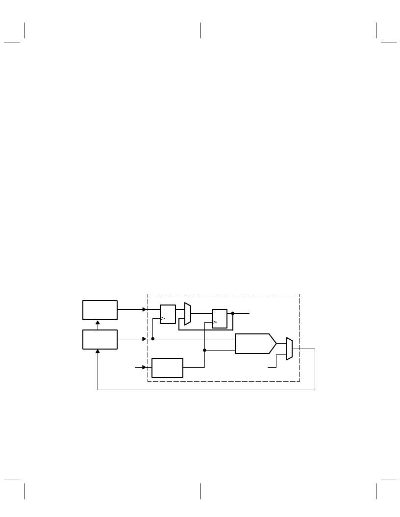
Figure 2–2 illustrates the pixel data latching structure and the operation of the loop clock PLL. The selected
clock source generates the dot clock which drives most of the digital logic of the TVP3026. The dot clock
is used as a reference frequency by the loop clock PLL and is subdivided as specified by the N value register.
The incoming LCLK is used as the other input of the PLL and is subdivided as specified by the M value
register. The PLL generates RCLK with the proper frequency and phase shift to phase align the divided dot
clock and divided LCLK. The pixel bus is latched on the rising edge of LCLK and then aligned with the internal
dot clock to synchronize with internal logic.
Loop Clock
PLL
D Q
D Q
LCLK
Dot Clock
Generator
Dot
Clock
Input Data Latch Structure
TVP3026
RCLK
CLKx
LCLK
P(63–0)
Graphics
Accelerator
VRAM
From Pixel Clock PLL
Figure 2–2. Loop Clock PLL Operation
The bit assignments of the N-, M-, and P-value and the status register for the loop clock PLL are shown in
Table 2–14. The bits shown as 0 or set to 1 must be written with these fixed values. When cleared to 0,
PLLEN disables the PLL and when set to 1, enables the PLL to oscillate. When reset to 1,the LOCK status
bit indicates that the PLL has locked to the selected frequency. The remaining status register bits are for
test purposes.
相關(guān)PDF資料 |
PDF描述 |
|---|---|
| TVP3026-250 | Video Interface PALETTE Exract(組合像素模式視頻接口調(diào)色器) |
| TX24 | 60.8 MM 5 X 8 DOT MATRIX DISPLAYS |
| TXB0102DCTR | 2-BIT BIDIRECTIONAL VOLTAGE-LEVEL TRANSLATOR WITH AUTO DIRECTION SENSING AND 【15-kV ESD PROTECTION |
| TXB0102DCTT | 2-BIT BIDIRECTIONAL VOLTAGE-LEVEL TRANSLATOR WITH AUTO DIRECTION SENSING AND 【15-kV ESD PROTECTION |
| TZX7V5D | surface mount silicon Zener diodes |
相關(guān)代理商/技術(shù)參數(shù) |
參數(shù)描述 |
|---|---|
| TVP3026-220AMDN | 制造商:TI 制造商全稱:Texas Instruments 功能描述:Video Interface Palette |
| TVP3026-220APCE | 制造商:TI 制造商全稱:Texas Instruments 功能描述:Video Interface Palette |
| TVP3026-220BMDN | 制造商:TI 制造商全稱:Texas Instruments 功能描述:Video Interface Palette |
| TVP3026-220BPCE | 制造商:Rochester Electronics LLC 功能描述:- Bulk |
| TVP3026-220MDN | 制造商:未知廠家 制造商全稱:未知廠家 功能描述:Video DAC with Color Palette (RAMDAC) |
發(fā)布緊急采購(gòu),3分鐘左右您將得到回復(fù)。