- 您現(xiàn)在的位置:買賣IC網(wǎng) > PDF目錄384032 > TVP3026-220 (Texas Instruments, Inc.) Video Interface PALETTE Exract(組合像素模式視頻接口調(diào)色器) PDF資料下載
參數(shù)資料
| 型號(hào): | TVP3026-220 |
| 廠商: | Texas Instruments, Inc. |
| 英文描述: | Video Interface PALETTE Exract(組合像素模式視頻接口調(diào)色器) |
| 中文描述: | 視頻接口調(diào)色板Exract(組合像素模式視頻接口調(diào)色器) |
| 文件頁數(shù): | 27/107頁 |
| 文件大小: | 707K |
| 代理商: | TVP3026-220 |
第1頁第2頁第3頁第4頁第5頁第6頁第7頁第8頁第9頁第10頁第11頁第12頁第13頁第14頁第15頁第16頁第17頁第18頁第19頁第20頁第21頁第22頁第23頁第24頁第25頁第26頁當(dāng)前第27頁第28頁第29頁第30頁第31頁第32頁第33頁第34頁第35頁第36頁第37頁第38頁第39頁第40頁第41頁第42頁第43頁第44頁第45頁第46頁第47頁第48頁第49頁第50頁第51頁第52頁第53頁第54頁第55頁第56頁第57頁第58頁第59頁第60頁第61頁第62頁第63頁第64頁第65頁第66頁第67頁第68頁第69頁第70頁第71頁第72頁第73頁第74頁第75頁第76頁第77頁第78頁第79頁第80頁第81頁第82頁第83頁第84頁第85頁第86頁第87頁第88頁第89頁第90頁第91頁第92頁第93頁第94頁第95頁第96頁第97頁第98頁第99頁第100頁第101頁第102頁第103頁第104頁第105頁第106頁第107頁
2–13
The N-, M-, and P-value registers may be programmed to any value within the following limits.
1
1
0
N(5–0)
M(5–0)
P(1,0)
62
62
3
LESEN enables the LCLK edge synchronizer function and should be set to 1 whenever a packed-24 mode
is used. In the packed-24 modes, only one LCLK rising edge per pixel group is aligned with the internal dot
clock. For example, in 8:3 packed-24 mode, only one of the three LCLKs is aligned to the internal dot clock.
The LCLK edge synchronizer function allows selection of which LCLK edge in the sequence of pixel bus
words is aligned with the internal dot clock. For each packed-24 mode there is an optimum setting for the
LCLK edge synchonizer delay LES1 and LES0. See Table 2–15 and subsection 2.6.6, Packed-24 Mode
for more details.
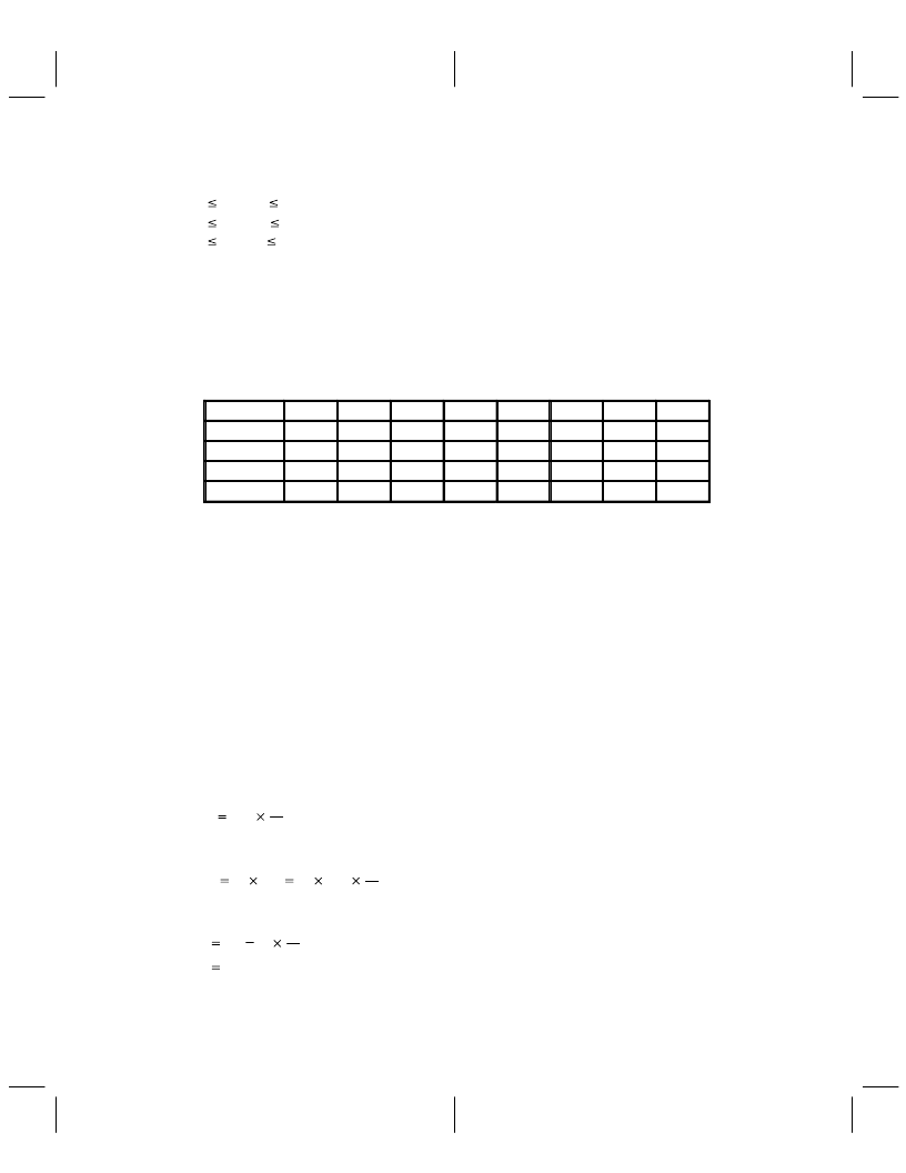
Table 2–14. Loop Clock PLL Registers
REGISTER
BIT 7
BIT 6
BIT 5
BIT 4
BIT 3
BIT 2
BIT 1
BIT 0
N value
1
1
N5
N4
N3
N2
N1
N0
M value
LES1
LES0
M5
M4
M3
M2
M1
M0
P value
PLLEN
1
1
1
LESEN
0
P1
P0
Status
X
LOCK
X
X
X
X
X
X
X = do not care
2.4.3.1
For all modes except packed-24, programming of the loop clock PLL registers depends on the system
configuration, pixel rate, color depth and pixel bus width. In addition, the internal VCO must be within its
operating range of 110 MHz to 220 MHz for the required RCLK output frequency. To determine the proper
M, N, P, and Q register values one should know the following:
Programming for All Modes Except Packed-24
Dot clock frequency (MHz) (F
D
) – pixel rate
Bits/pixel (B) – bits/pixel including overlay fields
Pixel bus width (W) – total pixel bus width used for this mode
External division factor (K) – external frequency division between RCLK output and LCLK input
The dot clock frequency can either be generated by the on-chip pixel clock PLL or by an external clock
source. The following two parameters can be easily calculated from the above parameters.
LCLK frequency (MHz) (F
L
) – frequency at which the pixel bus is loaded by the TVP3026
RCLK frequency (MHz) (F
R
) – frequency at RCLK output terminal of TVP3026
The LCLK frequency is given by
FL
FD
B
W
(5)
The RCLK frequency is F
L
times the external divide factor. When no external divide factor, K = 1.
B
W
FR
K
FL
K
FD
(6)
The N and M values are set as follows:
N
65
4
W
B
M
61
The P and Q frequency dividers must be programmed so that the VCO is within its operating range. The
VCO frequency is post-scaled by the P-divider followed by the Q-divider. The P-divider register (P) can take
相關(guān)PDF資料 |
PDF描述 |
|---|---|
| TVP3026-250 | Video Interface PALETTE Exract(組合像素模式視頻接口調(diào)色器) |
| TX24 | 60.8 MM 5 X 8 DOT MATRIX DISPLAYS |
| TXB0102DCTR | 2-BIT BIDIRECTIONAL VOLTAGE-LEVEL TRANSLATOR WITH AUTO DIRECTION SENSING AND 【15-kV ESD PROTECTION |
| TXB0102DCTT | 2-BIT BIDIRECTIONAL VOLTAGE-LEVEL TRANSLATOR WITH AUTO DIRECTION SENSING AND 【15-kV ESD PROTECTION |
| TZX7V5D | surface mount silicon Zener diodes |
相關(guān)代理商/技術(shù)參數(shù) |
參數(shù)描述 |
|---|---|
| TVP3026-220AMDN | 制造商:TI 制造商全稱:Texas Instruments 功能描述:Video Interface Palette |
| TVP3026-220APCE | 制造商:TI 制造商全稱:Texas Instruments 功能描述:Video Interface Palette |
| TVP3026-220BMDN | 制造商:TI 制造商全稱:Texas Instruments 功能描述:Video Interface Palette |
| TVP3026-220BPCE | 制造商:Rochester Electronics LLC 功能描述:- Bulk |
| TVP3026-220MDN | 制造商:未知廠家 制造商全稱:未知廠家 功能描述:Video DAC with Color Palette (RAMDAC) |
發(fā)布緊急采購,3分鐘左右您將得到回復(fù)。