- 您現(xiàn)在的位置:買賣IC網(wǎng) > PDF目錄383723 > OR3TP12 Field-Programmable System Chip (FPSC) Embedded Master/Target PCI Interface PDF資料下載
參數(shù)資料
| 型號(hào): | OR3TP12 |
| 英文描述: | Field-Programmable System Chip (FPSC) Embedded Master/Target PCI Interface |
| 中文描述: | 現(xiàn)場(chǎng)可編程系統(tǒng)芯片(促進(jìn)文化基金)嵌入式主/目標(biāo)PCI接口 |
| 文件頁數(shù): | 120/128頁 |
| 文件大小: | 2450K |
| 代理商: | OR3TP12 |
第1頁第2頁第3頁第4頁第5頁第6頁第7頁第8頁第9頁第10頁第11頁第12頁第13頁第14頁第15頁第16頁第17頁第18頁第19頁第20頁第21頁第22頁第23頁第24頁第25頁第26頁第27頁第28頁第29頁第30頁第31頁第32頁第33頁第34頁第35頁第36頁第37頁第38頁第39頁第40頁第41頁第42頁第43頁第44頁第45頁第46頁第47頁第48頁第49頁第50頁第51頁第52頁第53頁第54頁第55頁第56頁第57頁第58頁第59頁第60頁第61頁第62頁第63頁第64頁第65頁第66頁第67頁第68頁第69頁第70頁第71頁第72頁第73頁第74頁第75頁第76頁第77頁第78頁第79頁第80頁第81頁第82頁第83頁第84頁第85頁第86頁第87頁第88頁第89頁第90頁第91頁第92頁第93頁第94頁第95頁第96頁第97頁第98頁第99頁第100頁第101頁第102頁第103頁第104頁第105頁第106頁第107頁第108頁第109頁第110頁第111頁第112頁第113頁第114頁第115頁第116頁第117頁第118頁第119頁當(dāng)前第120頁第121頁第122頁第123頁第124頁第125頁第126頁第127頁第128頁
ORCAOR3TP12 FPSC
Embedded Master/Target PCI Interface
Data Sheet
March 2000
120
L Lucent Technologies Inc.
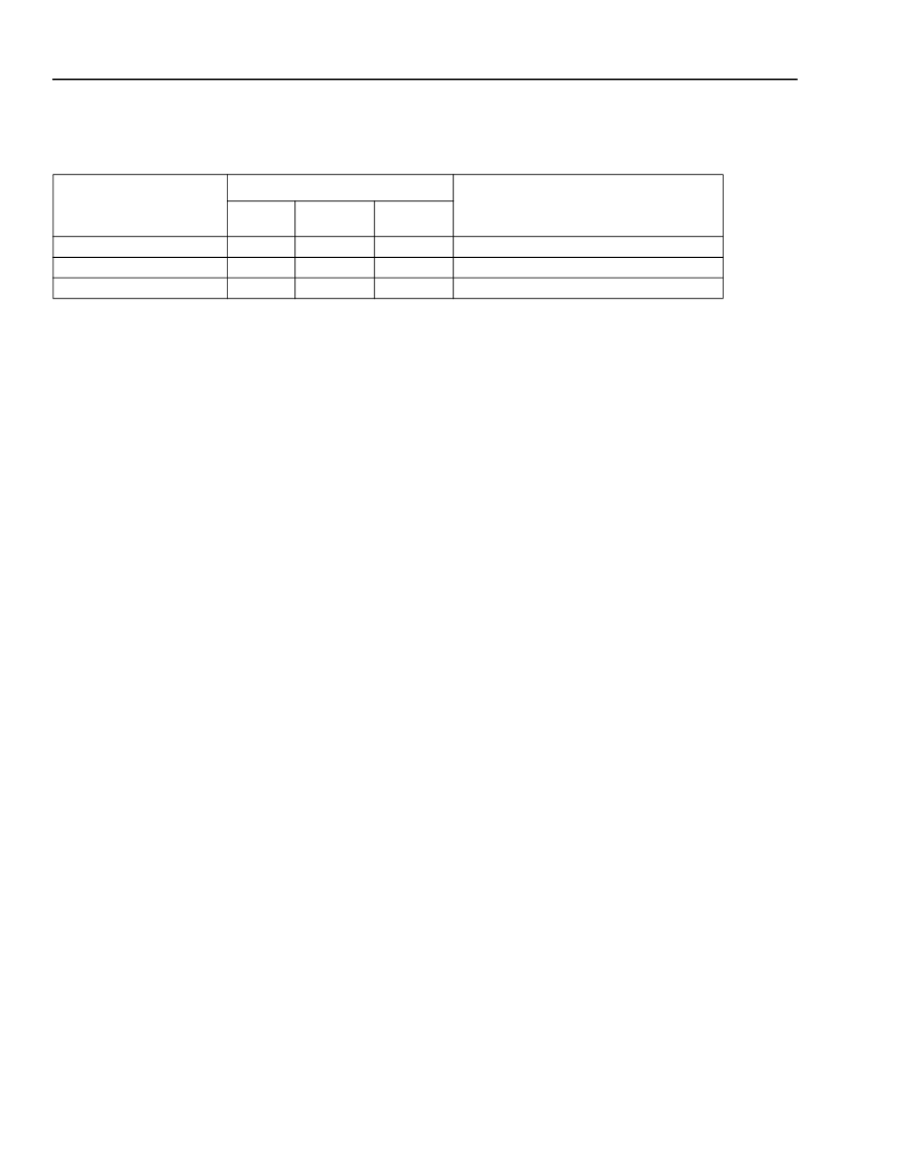
Package Thermal Characteristics
Table 45. ORCAOR3TP12 Plastic Package Thermal Guidelines
1. Mounted on a 4-layer JEDEC standard test board with two power/ground planes.
2. With thermal balls connected to board ground plane.
3. The value of y
JC
for all packages is <1 °C/W.
Package Coplanarity
The coplanarity limits of the ORCA Series 3/3+ packages are as follows:
I
PBGA: 8.0 mils
I
SQFP2: 3.15 mils
Package Parasitics
The electrical performance of an IC package, such as signal quality and noise sensitivity, is directly affected by the
package parasitics. Table 46 lists eight parasitics associated with the ORCA packages. These parasitics represent
the contributions of all components of a package, which include the bond wires, all internal package routing, and
the external leads.
Four inductances in nH are listed: L
SW
and L
SL,
the self-inductance of the lead; and L
MW
and L
ML
, the mutual
inductance to the nearest neighbor lead. These parameters are important in determining ground bounce noise and
inductive crosstalk noise. Three capacitances in pF are listed: C
M
, the mutual capacitance of the lead to the near-
est neighbor lead; and C
1
and C
2
, the total capacitance of the lead to all other leads (all other leads are assumed to
be grounded). These parameters are important in determining capacitive crosstalk and the capacitive loading effect
of the lead. Resistance values are in MW.
The parasitic values in Table 46 are for the circuit model of bond wire and package lead parasitics. If the mutual
capacitance value is not used in the designer’s model, then the value listed as mutual capacitance should be added
to each of the C
1
and C
2
capacitors.
Package
1
Θ
JA
(
°
C/W)
T
A
= 70
°
C Max
T
J
= 125
°
C Max
0 fpm (W)
4.2
2.4
2.9
0 fpm
200 fpm
500 fpm
240-Pin SQFP2
2
256-Pin PBGA
2, 3
352-Pin PBGA
2, 3
13.0
22.5
19.0
10.0
19.0
16.0
9.0
17.5
15.0
相關(guān)PDF資料 |
PDF描述 |
|---|---|
| OR62 | OR62 is a 6-input OR gate with 2x drive strength |
| OR73 | 7-input OR gate with 3x drive strength. |
| OR8GU41 | DIFFUSED TYPE (HIGH SPEED RECTIFIER APPLICATIONS) |
| ORCAORT4622 | Field-Programmable System Chip (FPSC) Four-Channel x 622 Mbits/s Backplane Transceiver |
| ORCAORT82G5 | 1.0?.25/2.0?.5/3.125 Gbits/s Backplane Interface FPSC |
相關(guān)代理商/技術(shù)參數(shù) |
參數(shù)描述 |
|---|---|
| OR3TP12-6BA256 | 制造商:未知廠家 制造商全稱:未知廠家 功能描述:User Programmable Special Function ASIC |
| OR3TP126BA256-DB | 功能描述:FPGA - 現(xiàn)場(chǎng)可編程門陣列 2016 LUT 187 I/O RoHS:否 制造商:Altera Corporation 系列:Cyclone V E 柵極數(shù)量: 邏輯塊數(shù)量:943 內(nèi)嵌式塊RAM - EBR:1956 kbit 輸入/輸出端數(shù)量:128 最大工作頻率:800 MHz 工作電源電壓:1.1 V 最大工作溫度:+ 70 C 安裝風(fēng)格:SMD/SMT 封裝 / 箱體:FBGA-256 |
| OR3TP12-6BA256I | 制造商:未知廠家 制造商全稱:未知廠家 功能描述:User Programmable Special Function ASIC |
| OR3TP126BA256I-DB | 功能描述:FPGA - 現(xiàn)場(chǎng)可編程門陣列 2016 LUT 187 I/O RoHS:否 制造商:Altera Corporation 系列:Cyclone V E 柵極數(shù)量: 邏輯塊數(shù)量:943 內(nèi)嵌式塊RAM - EBR:1956 kbit 輸入/輸出端數(shù)量:128 最大工作頻率:800 MHz 工作電源電壓:1.1 V 最大工作溫度:+ 70 C 安裝風(fēng)格:SMD/SMT 封裝 / 箱體:FBGA-256 |
| OR3TP12-6BA352 | 制造商:未知廠家 制造商全稱:未知廠家 功能描述:User Programmable Special Function ASIC |
發(fā)布緊急采購(gòu),3分鐘左右您將得到回復(fù)。