- 您現(xiàn)在的位置:買賣IC網(wǎng) > PDF目錄98080 > SII3124ACBHU PCI BUS CONTROLLER, PBGA364 PDF資料下載
參數(shù)資料
| 型號(hào): | SII3124ACBHU |
| 元件分類: | 總線控制器 |
| 英文描述: | PCI BUS CONTROLLER, PBGA364 |
| 封裝: | 21 X 21 MM, 1 MM PITCH, GREEN, BGA-364 |
| 文件頁數(shù): | 13/88頁 |
| 文件大小: | 592K |
| 代理商: | SII3124ACBHU |
第1頁第2頁第3頁第4頁第5頁第6頁第7頁第8頁第9頁第10頁第11頁第12頁當(dāng)前第13頁第14頁第15頁第16頁第17頁第18頁第19頁第20頁第21頁第22頁第23頁第24頁第25頁第26頁第27頁第28頁第29頁第30頁第31頁第32頁第33頁第34頁第35頁第36頁第37頁第38頁第39頁第40頁第41頁第42頁第43頁第44頁第45頁第46頁第47頁第48頁第49頁第50頁第51頁第52頁第53頁第54頁第55頁第56頁第57頁第58頁第59頁第60頁第61頁第62頁第63頁第64頁第65頁第66頁第67頁第68頁第69頁第70頁第71頁第72頁第73頁第74頁第75頁第76頁第77頁第78頁第79頁第80頁第81頁第82頁第83頁第84頁第85頁第86頁第87頁第88頁
PCI-X to Serial ATA Controller
Data Sheet
Silicon Image, Inc.
2006 Silicon Image, Inc.
SiI-DS-0160-C
20
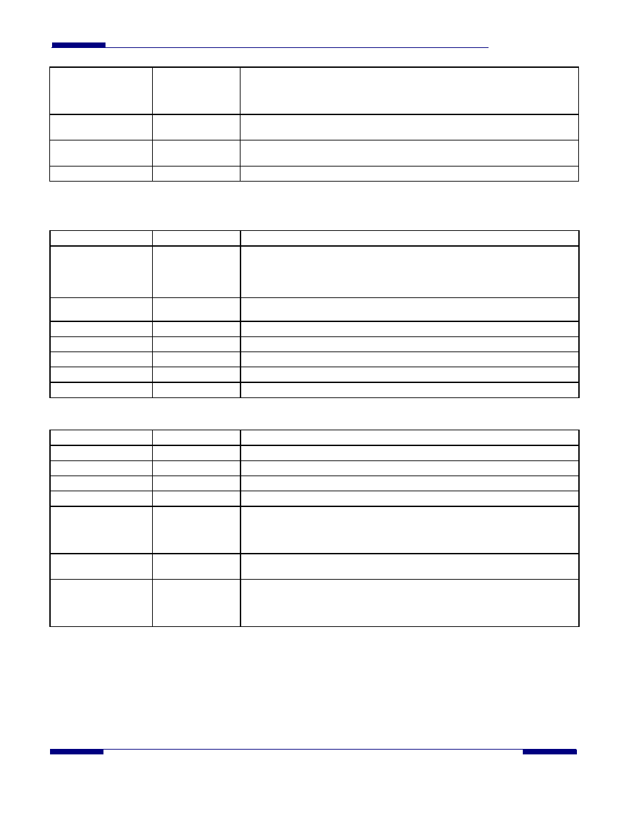
PCI_INTA_N,
PCI_INTB_N,
PCI_INTC_N,
PCI_INTD_N
V5, W5, W6, Y6
Interrupt. PCI_INTA_N is asserted to request a system interrupt. The other
interrupt pins may be enabled by means outside that specified by the PCI
specification (see description for Port Interrupt Enable register).
PCI_CLK
U1
Clock. PCI_CLK is the reference clock for all PCI interface signals except
PCI_RST_N and PCI_INTA_N.
PCI_RST_N
U6
Reset. PCI_RST_N initializes the PCI interface and sets internal registers to
their initial state. All PCI outputs are tri-stated while PCI_RST_N is active.
M66EN
T20
PCI 66 MHz Enable.
3.3.2
Flash / I
2C Pins
Signal Name
Pin Number(s)
Description
FL_ADDR[18:00]
D7, B7, A7, D8, B8,
A8, D9, B9, A9, D10,
B10, A10, D11, B11,
A11, D12, B12, A12,
D13
Flash Address. FL_ ADDR[18:00] is the Flash Memory address for up to 512K
of Flash Memory.
FL_DATA[07:00]
B13, A13, D14, B14,
A14, D15, B15, A15
Flash Data. 8-bit Flash memory data bus
FL_RD_N
A6
Flash Read Enable. Active low
FL_WR_N
B6
Flash Write Enable. Active low
FL_CS_N
D6
Flash Chip Select. Active low
I2C_SDAT
D5
I
2C Serial Data. Serial Interface (I2C) data line
I2C_SCLK
B5
I
2C Serial Clock. Serial Interface (I2C) clock
3.3.3
Serial ATA Signals
Signal Name
Pin Number(s)
Description
Rx[3:0]+
C1, F1, L1, P1
Receive +. Serial receiver differential signal, positive side.
Rx[3:0]-
C2, F2, L2, P2
Receive -. Serial receiver differential signal, negative side.
Tx[3:0]+
D2, G2, M2, R2
Transmit +. Serial transmitter differential signal, positive side.
Tx[3:0]-
D1, G1, M1, R1
Transmit -. Serial transmitter differential signal, negative side.
XTALI/CLKI
J1
Crystal In. Crystal oscillator pin for SerDes reference clock. When external
clock source is selected, the external clock (either 25MHz or 100 MHz) will
come in through this pin. The clock must be 1.8V swing and the precision
recommendation is ±50ppm.
XTALO
J2
Crystal Out. Crystal oscillator pin for SerDes reference clock. A 25MHz crystal
must be used.
REXT
J4
External Reference. External reference resistor pin for termination calibration.
This pin provides the additional function of selecting frequency of the clock
source. For 25MHz, a 1K, 1% resistor is connected to ground. For 100MHz, a
4.99K, 1% resistor is connected to ground.
相關(guān)PDF資料 |
PDF描述 |
|---|---|
| SII3512ECTU128 | PCI BUS CONTROLLER, PQFP128 |
| SII3531ACNU | PCI BUS CONTROLLER, QCC48 |
| SIO10N268-NU | MULTIFUNCTION PERIPHERAL, PQFP128 |
| SIS300 | GRAPHICS PROCESSOR, PBGA365 |
| SK12430PJT | 800 MHz, OTHER CLOCK GENERATOR, PQCC28 |
相關(guān)代理商/技術(shù)參數(shù) |
參數(shù)描述 |
|---|---|
| SII3132 | 制造商:SILICONIMAGE 制造商全稱:SILICONIMAGE 功能描述:PCI Express to 2-Port Serial ATA II Host Controller |
| SII3132CNU | 制造商:Silicon Image Inc 功能描述:PCI Express to Serial ATA Controller 88-Pin QFN |
| SII3512 | 制造商:SILICONIMAGE 制造商全稱:SILICONIMAGE 功能描述:PCI to Serial ATA Controller |
| SII3512ECTU128 | 制造商:Silicon Image Inc 功能描述:PCI to Serial ATA Controller 128-Pin TQFP 制造商:Silicone Image 功能描述: |
| SII3531 | 制造商:SILICONIMAGE 制造商全稱:SILICONIMAGE 功能描述:SteelVine⑩ Host Controller |
發(fā)布緊急采購(gòu),3分鐘左右您將得到回復(fù)。