- 您現在的位置:買賣IC網 > PDF目錄1958 > ORT8850L-3BM680C (Lattice Semiconductor Corporation)IC FPSC TRANSCEIVER 8CH 680-BGA PDF資料下載
參數資料
| 型號: | ORT8850L-3BM680C |
| 廠商: | Lattice Semiconductor Corporation |
| 文件頁數: | 82/105頁 |
| 文件大?。?/td> | 0K |
| 描述: | IC FPSC TRANSCEIVER 8CH 680-BGA |
| 產品變化通告: | Product Discontinuation 01/Aug/2011 |
| 標準包裝: | 24 |
| 系列: | * |
第1頁第2頁第3頁第4頁第5頁第6頁第7頁第8頁第9頁第10頁第11頁第12頁第13頁第14頁第15頁第16頁第17頁第18頁第19頁第20頁第21頁第22頁第23頁第24頁第25頁第26頁第27頁第28頁第29頁第30頁第31頁第32頁第33頁第34頁第35頁第36頁第37頁第38頁第39頁第40頁第41頁第42頁第43頁第44頁第45頁第46頁第47頁第48頁第49頁第50頁第51頁第52頁第53頁第54頁第55頁第56頁第57頁第58頁第59頁第60頁第61頁第62頁第63頁第64頁第65頁第66頁第67頁第68頁第69頁第70頁第71頁第72頁第73頁第74頁第75頁第76頁第77頁第78頁第79頁第80頁第81頁當前第82頁第83頁第84頁第85頁第86頁第87頁第88頁第89頁第90頁第91頁第92頁第93頁第94頁第95頁第96頁第97頁第98頁第99頁第100頁第101頁第102頁第103頁第104頁第105頁
Lattice Semiconductor
ORCA ORT8850 Data Sheet
78
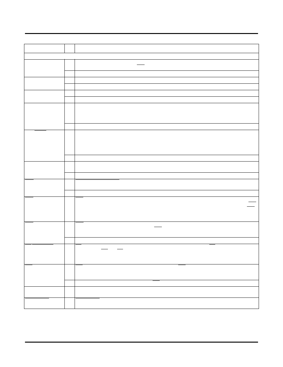
Special-Purpose Pins
M[3:0]
I
During power-up and initialization, M0—M3 are used to select the conguration mode with their val-
ues latched on the rising edge of INIT. During conguration, a pull-up is enabled.
I/O After conguration, these pins are user-programmable I/O.*
PLL_CK[0:7][TC]
I
Semi-dedicated PLL clock pins. During conguration they are 3-stated with a pull up.
I/O These pins are user-programmable I/O pins if not used by PLLs after conguration.
P[TBLR]CLK[1:0][T
C]
I
Pins dedicated for the primary clock. Input pins on the middle of each side with differential pairing.
I/O After conguration these pins are user-programmable I/O, if not used for clock inputs.
TDI, TCK, TMS
I
If boundary-scan is used, these pins are test data in, test clock, and test mode select inputs. If
boundary-scan is not selected, all boundary-scan functions are inhibited once conguration is com-
plete. Even if boundary-scan is not used, either TCK or TMS must be held at logic 1 during congu-
ration. Each pin has a pull-up enabled during conguration.
I/O After conguration, these pins are user-programmable I/O in boundary scan is not used.*
RDY/BUSY/RCLK
O
During conguration in asynchronous peripheral mode, RDY/RCLK indicates another byte can be
written to the FPGA. If a read operation is done when the device is selected, the same status is also
available on D7 in asynchronous peripheral mode.
During the master parallel conguration mode, RCLK is a read output signal to an external memory.
This output is not normally used.
I/O After conguration this pin is a user-programmable I/O pin.*
HDC
O
High during conguration is output high until conguration is complete. It is used as a control output,
indicating that conguration is not complete.
I/O After conguration, this pin is a user-programmable I/O pin.*
LDC
O
Low during conguration
is output low until conguration is complete. It is used as a control output,
indicating that conguration is not complete.
I/O After conguration, this pin is a user-programmable I/O pin.*
INIT
I/O
INIT
is a bidirectional signal before and during conguration. During conguration, a pull-up is
enabled, but an external pull-up resistor is recommended. As an active-low open-drain output, INIT
is held low during power stabilization and internal clearing of memory. As an active-low input, INIT
holds the FPGA in the wait-state before the start of conguration.
After conguration, this pin is a user-programmable I/O pin.*
CS0, CS1
I
CS0
and CS1 are used in the asynchronous peripheral, slave parallel, and microprocessor congu-
ration modes. The FPGA is selected when CS0 is low and CS1 is high. During conguration, a pull-
up is enabled.
I/O After conguration, if MPI is not used, these pins are user-programmable I/O pins.*
RD/MPI_STRB
I
RD
is used in the asynchronous peripheral conguration mode. A low on RD changes D[7:3] into a
status output. WR and RD should not be used simultaneously. If they are, the write strobe overrides.
This pin is also used as the
MPI data transfer strobe. As a status indication, a high indicates ready,
and a low indicates busy.
WR/MPI_RW
I
WR is used in asynchronous peripheral mode. A low on WR transfers data on D[7:0] to the FPGA.
In MPI mode, a high on MPI_RW allows a read from the data bus, while a low causes a write trans-
fer to the FPGA.
I/O After conguration, if the MPI is not used, WR/MPI_RW is a user-programmable I/O pin.*
PPC_A[14:31]
I
During MPI mode the PPC_A[14:31] are used as the address bus driven by the
PowerPC bus mas-
ter utilizing the least-signicant bits of the
PowerPC 32-bit address.
MPI_BURST
I
MPI_BURST is driven low to indicate a burst transfer is in progress in MPI mode. Driven high indi-
cates that the current transfer is not a burst.
Table 32. FPGA Common-Function Pin Descriptions (Continued)
Symbol
I/O
Description
1. The FPGA States of Operation section contains more information on how to control these signals during start-up. The timing of DONE
release is controlled by one set of bit stream options, and the timing of the simultaneous release of all other conguration pins (and the activa-
tion of all user I/Os) is controlled by a second set of options.
相關PDF資料 |
PDF描述 |
|---|---|
| P1010PSE5HFA | MPU PROTO 800/667 425-TEPBGA1 |
| P1013NXN2LFB | IC MPU 1067MHZ 689TEPBGA |
| P1013PSE2EFA | IC MPU PROTO 600MHZ 689-TEPBGA |
| P1014NSN5DFA | IC MPU 800MHZ 425TEPBGA1 |
| P1014NSN5FFA | IC MPU 800MHZ 425TEPBGA1 |
相關代理商/技術參數 |
參數描述 |
|---|---|
| ORT8850L-3BMN680C | 功能描述:FPGA - 現場可編程門陣列 4992 LUT 278 I/O RoHS:否 制造商:Altera Corporation 系列:Cyclone V E 柵極數量: 邏輯塊數量:943 內嵌式塊RAM - EBR:1956 kbit 輸入/輸出端數量:128 最大工作頻率:800 MHz 工作電源電壓:1.1 V 最大工作溫度:+ 70 C 安裝風格:SMD/SMT 封裝 / 箱體:FBGA-256 |
| ORT9303 | 制造商:BOT 制造商全稱:Bedford Opto Technology Ltd. 功能描述:3 ELEMENT PCB MOUNT 1.8mm LED ARRAY |
| ORT9303B | 制造商:BOT 制造商全稱:Bedford Opto Technology Ltd. 功能描述:3 ELEMENT PCB MOUNT 1.8mm LED ARRAY |
| ORT9303BL | 制造商:BOT 制造商全稱:Bedford Opto Technology Ltd. 功能描述:3 ELEMENT PCB MOUNT 1.8mm LED ARRAY |
| ORT9303G | 制造商:BOT 制造商全稱:Bedford Opto Technology Ltd. 功能描述:3 ELEMENT PCB MOUNT 1.8mm LED ARRAY |
發(fā)布緊急采購,3分鐘左右您將得到回復。