- 您現(xiàn)在的位置:買賣IC網(wǎng) > PDF目錄1958 > ORT8850L-3BM680C (Lattice Semiconductor Corporation)IC FPSC TRANSCEIVER 8CH 680-BGA PDF資料下載
參數(shù)資料
| 型號: | ORT8850L-3BM680C |
| 廠商: | Lattice Semiconductor Corporation |
| 文件頁數(shù): | 39/105頁 |
| 文件大小: | 0K |
| 描述: | IC FPSC TRANSCEIVER 8CH 680-BGA |
| 產(chǎn)品變化通告: | Product Discontinuation 01/Aug/2011 |
| 標(biāo)準(zhǔn)包裝: | 24 |
| 系列: | * |
第1頁第2頁第3頁第4頁第5頁第6頁第7頁第8頁第9頁第10頁第11頁第12頁第13頁第14頁第15頁第16頁第17頁第18頁第19頁第20頁第21頁第22頁第23頁第24頁第25頁第26頁第27頁第28頁第29頁第30頁第31頁第32頁第33頁第34頁第35頁第36頁第37頁第38頁當(dāng)前第39頁第40頁第41頁第42頁第43頁第44頁第45頁第46頁第47頁第48頁第49頁第50頁第51頁第52頁第53頁第54頁第55頁第56頁第57頁第58頁第59頁第60頁第61頁第62頁第63頁第64頁第65頁第66頁第67頁第68頁第69頁第70頁第71頁第72頁第73頁第74頁第75頁第76頁第77頁第78頁第79頁第80頁第81頁第82頁第83頁第84頁第85頁第86頁第87頁第88頁第89頁第90頁第91頁第92頁第93頁第94頁第95頁第96頁第97頁第98頁第99頁第100頁第101頁第102頁第103頁第104頁第105頁
Lattice Semiconductor
ORCA ORT8850 Data Sheet
39
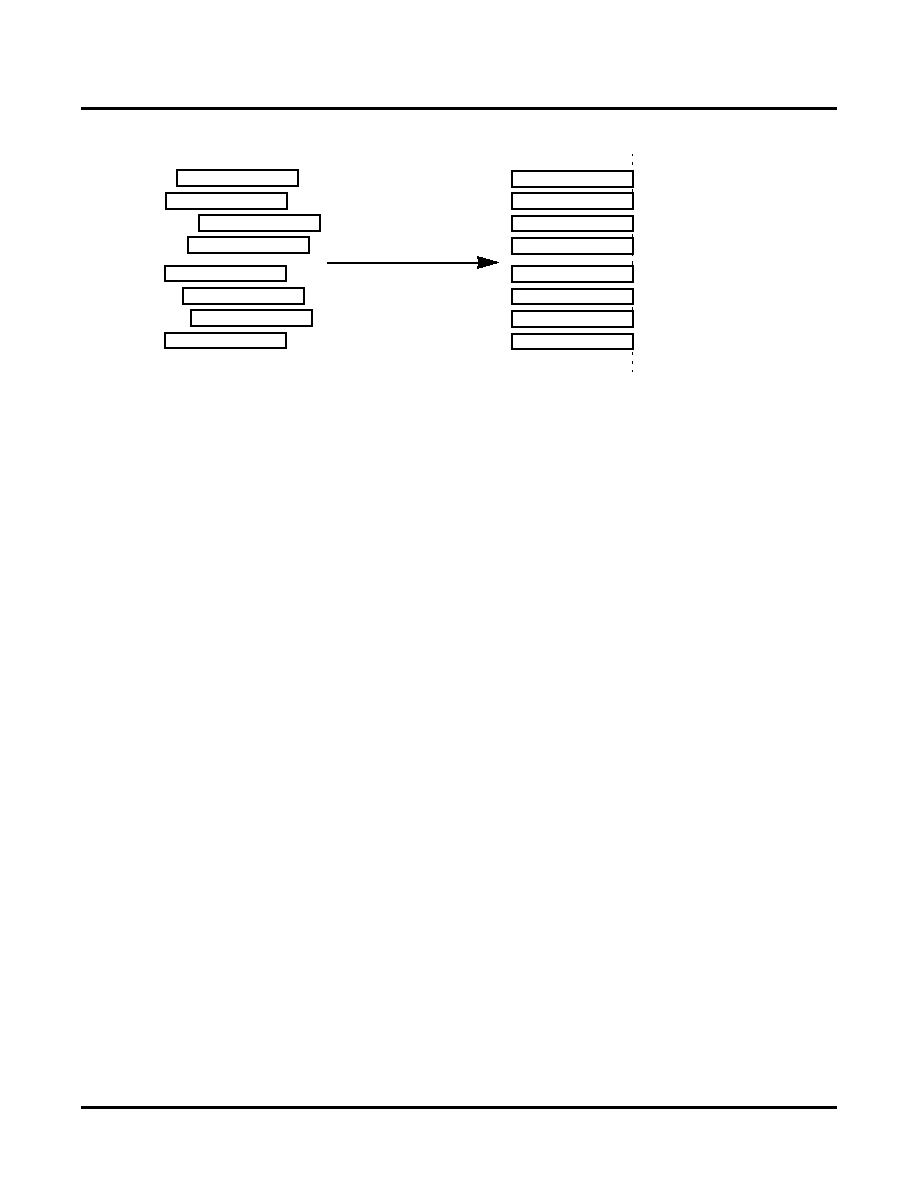
Figure 20. Alignment of all Eight SERDES Channels.
There is a provision to allow certain streams to be disabled (i.e. not producing alarms or affecting synchronization).
These streams can be enabled at a later time without disrupting other streams. If the newly enabled stream needs
to be a part of a bigger group the entire group must be resynchronized unless the affected stream was active when
the initial synchronization was performed. As long as all streams to be aligned were active when the most recent
synchronization was performed, individual streams may be enabled or disabled without affecting synchronization.
It is recommended that users select the smallest possible groups for channel alignment. If an application only
requires that two channels be aligned then it is best to use by-2 grouping. All of the channels in a group will affect
the group’s total alignment. If a channel in a group fails or is shut down it will not affect any of the other channels in
the group. This channel will simply be removed from the alignment algorithm. When the channel is re-enabled into
a working group it will be out of alignment with the rest of the group. It will be necessary to perform a FIFO realign-
ment procedure to realign the group. During a FIFO realignment data will not pass through any of the channels in
the alignment group.
Alignment FIFO Algorithm
The algorithm controlling writes to the alignment FIFO and reads from it operates as follows: Prior to detecting the
rst frame pulse for a link being aligned, each link in the group continually writes to address 0 within its own FIFO
(each link has a FIFO). When the rst link in the group receives a frame pulse from Framer block the write pointer
for the corresponding FIFO increments to next write address on each clock cycle. L inks that have not received a
frame pulse continue to write into their respective FIFOs. When any link receives a frame pulse, the write address
for that FIFO will be reset to ‘0’
The operation of the alignment algorithm requires a wait of several clocks from the rst arriving frame pulse before
reading of FIFO data begins. In this case, when all frame pulses arrive together the alignment algorithm initiates
reads after 9 clocks cycles. If, however, the rst to last arriving frame pulses are separated by multiple clock cycles,
there will be additional clock cycles between the rst frame pulse and the rst read. If all links in the group have not
reported a valid frame pulse signal after 18 clock cycles, an out of sync state is entered and an alarm is generated.
After all links have received frame pulses and are incrementing their write addresses while writing into their FIFOs,
data is then read out of each link's FIFO one byte at a time. All aligned links are now Frame/byte/bit synchronous.
FIFO Alignment Procedure
The FIFO alignment block has the ability to be realigned by changing the value of bits in the alignment control reg-
isters. This may be done in the FPGA logic or under the control of an external device through the system bus or
MPI. Alignment must take place after the stream has settled with valid data to guarantee proper channel alignment
and uncorrupted data transmission.
Channel realignment must occur when a channel goes from the Out-Of-Frame (OOF) state to the In-Frame state.
This happens when the channels are rst powered up and given a valid frame pulse. This is the obvious known
Channel AA
Channel AB
Channel AC
Channel AD
Channel BA
Channel BB
Channel BC
Channel BD
Channel AA
Channel AB
Channel AC
Channel AD
Channel BA
Channel BB
Channel BC
Channel BD
t0
相關(guān)PDF資料 |
PDF描述 |
|---|---|
| P1010PSE5HFA | MPU PROTO 800/667 425-TEPBGA1 |
| P1013NXN2LFB | IC MPU 1067MHZ 689TEPBGA |
| P1013PSE2EFA | IC MPU PROTO 600MHZ 689-TEPBGA |
| P1014NSN5DFA | IC MPU 800MHZ 425TEPBGA1 |
| P1014NSN5FFA | IC MPU 800MHZ 425TEPBGA1 |
相關(guān)代理商/技術(shù)參數(shù) |
參數(shù)描述 |
|---|---|
| ORT8850L-3BMN680C | 功能描述:FPGA - 現(xiàn)場可編程門陣列 4992 LUT 278 I/O RoHS:否 制造商:Altera Corporation 系列:Cyclone V E 柵極數(shù)量: 邏輯塊數(shù)量:943 內(nèi)嵌式塊RAM - EBR:1956 kbit 輸入/輸出端數(shù)量:128 最大工作頻率:800 MHz 工作電源電壓:1.1 V 最大工作溫度:+ 70 C 安裝風(fēng)格:SMD/SMT 封裝 / 箱體:FBGA-256 |
| ORT9303 | 制造商:BOT 制造商全稱:Bedford Opto Technology Ltd. 功能描述:3 ELEMENT PCB MOUNT 1.8mm LED ARRAY |
| ORT9303B | 制造商:BOT 制造商全稱:Bedford Opto Technology Ltd. 功能描述:3 ELEMENT PCB MOUNT 1.8mm LED ARRAY |
| ORT9303BL | 制造商:BOT 制造商全稱:Bedford Opto Technology Ltd. 功能描述:3 ELEMENT PCB MOUNT 1.8mm LED ARRAY |
| ORT9303G | 制造商:BOT 制造商全稱:Bedford Opto Technology Ltd. 功能描述:3 ELEMENT PCB MOUNT 1.8mm LED ARRAY |
發(fā)布緊急采購,3分鐘左右您將得到回復(fù)。