- 您現(xiàn)在的位置:買(mǎi)賣(mài)IC網(wǎng) > PDF目錄1958 > ORT8850L-3BM680C (Lattice Semiconductor Corporation)IC FPSC TRANSCEIVER 8CH 680-BGA PDF資料下載
參數(shù)資料
| 型號(hào): | ORT8850L-3BM680C |
| 廠商: | Lattice Semiconductor Corporation |
| 文件頁(yè)數(shù): | 14/105頁(yè) |
| 文件大?。?/td> | 0K |
| 描述: | IC FPSC TRANSCEIVER 8CH 680-BGA |
| 產(chǎn)品變化通告: | Product Discontinuation 01/Aug/2011 |
| 標(biāo)準(zhǔn)包裝: | 24 |
| 系列: | * |
第1頁(yè)第2頁(yè)第3頁(yè)第4頁(yè)第5頁(yè)第6頁(yè)第7頁(yè)第8頁(yè)第9頁(yè)第10頁(yè)第11頁(yè)第12頁(yè)第13頁(yè)當(dāng)前第14頁(yè)第15頁(yè)第16頁(yè)第17頁(yè)第18頁(yè)第19頁(yè)第20頁(yè)第21頁(yè)第22頁(yè)第23頁(yè)第24頁(yè)第25頁(yè)第26頁(yè)第27頁(yè)第28頁(yè)第29頁(yè)第30頁(yè)第31頁(yè)第32頁(yè)第33頁(yè)第34頁(yè)第35頁(yè)第36頁(yè)第37頁(yè)第38頁(yè)第39頁(yè)第40頁(yè)第41頁(yè)第42頁(yè)第43頁(yè)第44頁(yè)第45頁(yè)第46頁(yè)第47頁(yè)第48頁(yè)第49頁(yè)第50頁(yè)第51頁(yè)第52頁(yè)第53頁(yè)第54頁(yè)第55頁(yè)第56頁(yè)第57頁(yè)第58頁(yè)第59頁(yè)第60頁(yè)第61頁(yè)第62頁(yè)第63頁(yè)第64頁(yè)第65頁(yè)第66頁(yè)第67頁(yè)第68頁(yè)第69頁(yè)第70頁(yè)第71頁(yè)第72頁(yè)第73頁(yè)第74頁(yè)第75頁(yè)第76頁(yè)第77頁(yè)第78頁(yè)第79頁(yè)第80頁(yè)第81頁(yè)第82頁(yè)第83頁(yè)第84頁(yè)第85頁(yè)第86頁(yè)第87頁(yè)第88頁(yè)第89頁(yè)第90頁(yè)第91頁(yè)第92頁(yè)第93頁(yè)第94頁(yè)第95頁(yè)第96頁(yè)第97頁(yè)第98頁(yè)第99頁(yè)第100頁(yè)第101頁(yè)第102頁(yè)第103頁(yè)第104頁(yè)第105頁(yè)
Lattice Semiconductor
ORCA ORT8850 Data Sheet
16
this feature the alignment FIFO cannot be used with this clock architecture. The recovered clock is used for all
receive timing in the embedded core and supplied to the FPGA logic which must provide the clock domain transfer
functionality.
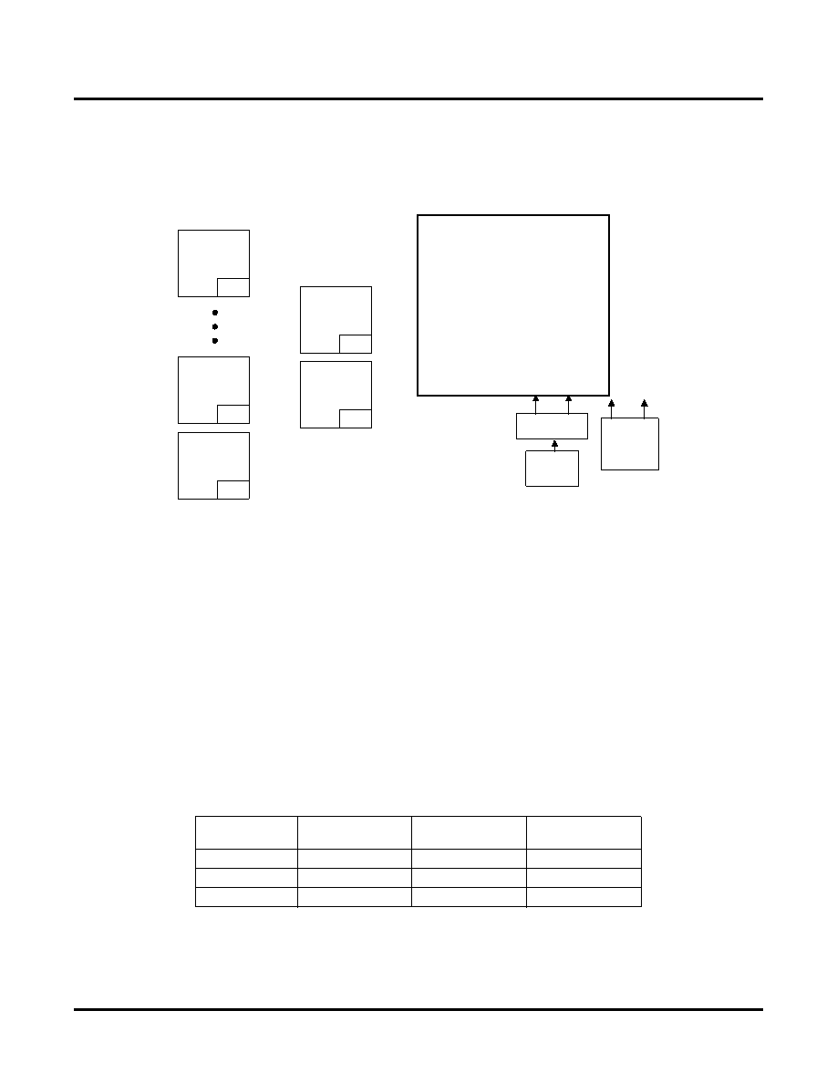
Figure 6. Independent Clock Architecture
SONET Bypass Mode
It is possible to utilize only the serializer and deserializer (SERDES) blocks in the ORT8850 and to bypass all of the
SONET framing and scrambling/descrambling. In this mode the parallel data from the FPGA is serialized and sent
out the LVDS pins. The serial data in the receive direction will be run through the SERDES and then received as
parallel data with a recovered clock into the FPGA.
In the SONET Bypass mode there exists half and quarter rate selection options. Half rate allows the SERDES to
operate at 4x the reference clock. When using half rate mode only the bits 7:4 of the parallel FPGA bus are utilized.
Quarter rate allows the SERDES to operate at 2x the reference clock. When using quarter rate mode only bits 7:6
of the parallel FPGA bus are utilized. Half rate and quarter rate are selectable per channel and can be mixed per
channel so that some channels can run in full rate mode while others operate in half rate mode and still others
operate in quarter rate mode.
As shown in Table 3, 63.00 MHz is the slowest reference clock and 106.25 MHz is the fastest reference clock fre-
quency supported. For all three modes, all bandwidths within the reference clock limits are supported. Note that
there are gaps between the bandwidths supported in the three modes.
Table 3. SONET Bypass Mode Bandwidth Options
In the SONET Bypass mode a 1's density function similar to SONET scrambling must be implemented in the FPGA
logic to assure reliable clock recovery at the receiver.
Reference Clock
Full Mode
Half Mode
Bits [7:4] Used
Quarter Mode
Bits [7:6] Used
63
504.00 Mbits/s
252.00 Mbits/s
126.00 Mbits/s
77.76
622.08Mbits/s
311.04Mbits/s
155.52Mbits/s
106.25
850.00 Mbits/s
425.00 Mbits/s
212.50 Mbits/s
Fabric
Cards
Port
Cards
System Diagram
Osc.
Board
Details
77.76 Mhz
Oscillator
SYS_CLK_P
SYS_CLK_N
* Examples of
Typical Board
Components
LVDS
Buffer
or
77.76 Mhz
Differential
Output
Oscillator
TI
SN65LVDS31D*
Conner
Winfield
HC54R8*
ORT8850
(SERDES at
622 Mbps)
相關(guān)PDF資料 |
PDF描述 |
|---|---|
| P1010PSE5HFA | MPU PROTO 800/667 425-TEPBGA1 |
| P1013NXN2LFB | IC MPU 1067MHZ 689TEPBGA |
| P1013PSE2EFA | IC MPU PROTO 600MHZ 689-TEPBGA |
| P1014NSN5DFA | IC MPU 800MHZ 425TEPBGA1 |
| P1014NSN5FFA | IC MPU 800MHZ 425TEPBGA1 |
相關(guān)代理商/技術(shù)參數(shù) |
參數(shù)描述 |
|---|---|
| ORT8850L-3BMN680C | 功能描述:FPGA - 現(xiàn)場(chǎng)可編程門(mén)陣列 4992 LUT 278 I/O RoHS:否 制造商:Altera Corporation 系列:Cyclone V E 柵極數(shù)量: 邏輯塊數(shù)量:943 內(nèi)嵌式塊RAM - EBR:1956 kbit 輸入/輸出端數(shù)量:128 最大工作頻率:800 MHz 工作電源電壓:1.1 V 最大工作溫度:+ 70 C 安裝風(fēng)格:SMD/SMT 封裝 / 箱體:FBGA-256 |
| ORT9303 | 制造商:BOT 制造商全稱(chēng):Bedford Opto Technology Ltd. 功能描述:3 ELEMENT PCB MOUNT 1.8mm LED ARRAY |
| ORT9303B | 制造商:BOT 制造商全稱(chēng):Bedford Opto Technology Ltd. 功能描述:3 ELEMENT PCB MOUNT 1.8mm LED ARRAY |
| ORT9303BL | 制造商:BOT 制造商全稱(chēng):Bedford Opto Technology Ltd. 功能描述:3 ELEMENT PCB MOUNT 1.8mm LED ARRAY |
| ORT9303G | 制造商:BOT 制造商全稱(chēng):Bedford Opto Technology Ltd. 功能描述:3 ELEMENT PCB MOUNT 1.8mm LED ARRAY |
發(fā)布緊急采購(gòu),3分鐘左右您將得到回復(fù)。