- 您現(xiàn)在的位置:買(mǎi)賣(mài)IC網(wǎng) > PDF目錄1958 > ORT8850L-3BM680C (Lattice Semiconductor Corporation)IC FPSC TRANSCEIVER 8CH 680-BGA PDF資料下載
參數(shù)資料
| 型號(hào): | ORT8850L-3BM680C |
| 廠商: | Lattice Semiconductor Corporation |
| 文件頁(yè)數(shù): | 50/105頁(yè) |
| 文件大小: | 0K |
| 描述: | IC FPSC TRANSCEIVER 8CH 680-BGA |
| 產(chǎn)品變化通告: | Product Discontinuation 01/Aug/2011 |
| 標(biāo)準(zhǔn)包裝: | 24 |
| 系列: | * |
第1頁(yè)第2頁(yè)第3頁(yè)第4頁(yè)第5頁(yè)第6頁(yè)第7頁(yè)第8頁(yè)第9頁(yè)第10頁(yè)第11頁(yè)第12頁(yè)第13頁(yè)第14頁(yè)第15頁(yè)第16頁(yè)第17頁(yè)第18頁(yè)第19頁(yè)第20頁(yè)第21頁(yè)第22頁(yè)第23頁(yè)第24頁(yè)第25頁(yè)第26頁(yè)第27頁(yè)第28頁(yè)第29頁(yè)第30頁(yè)第31頁(yè)第32頁(yè)第33頁(yè)第34頁(yè)第35頁(yè)第36頁(yè)第37頁(yè)第38頁(yè)第39頁(yè)第40頁(yè)第41頁(yè)第42頁(yè)第43頁(yè)第44頁(yè)第45頁(yè)第46頁(yè)第47頁(yè)第48頁(yè)第49頁(yè)當(dāng)前第50頁(yè)第51頁(yè)第52頁(yè)第53頁(yè)第54頁(yè)第55頁(yè)第56頁(yè)第57頁(yè)第58頁(yè)第59頁(yè)第60頁(yè)第61頁(yè)第62頁(yè)第63頁(yè)第64頁(yè)第65頁(yè)第66頁(yè)第67頁(yè)第68頁(yè)第69頁(yè)第70頁(yè)第71頁(yè)第72頁(yè)第73頁(yè)第74頁(yè)第75頁(yè)第76頁(yè)第77頁(yè)第78頁(yè)第79頁(yè)第80頁(yè)第81頁(yè)第82頁(yè)第83頁(yè)第84頁(yè)第85頁(yè)第86頁(yè)第87頁(yè)第88頁(yè)第89頁(yè)第90頁(yè)第91頁(yè)第92頁(yè)第93頁(yè)第94頁(yè)第95頁(yè)第96頁(yè)第97頁(yè)第98頁(yè)第99頁(yè)第100頁(yè)第101頁(yè)第102頁(yè)第103頁(yè)第104頁(yè)第105頁(yè)
Lattice Semiconductor
ORCA ORT8850 Data Sheet
49
Clock and Data Timing at the FPGA/Embedded Core Interface - SONET Block
(Note: This section assumes a basic understanding of the Lattice Semiconductor ispLEVER design tool set)
This section provides examples of the clock and data timing relationships at the FPGA/Embedded Core interface
for both the parallel SONET data and the serial TOH data. The initiation of a change of data is referred to as the
"launch" time and the actual time of capture of the data is referred to as the "capture" time. Two relationships are
discussed, the relationship between data and clock at the interface itself and the relative timing constraints on the
signals in the FPGA logic between the interface and the launch/capture latch in the FPGA portion of the FPSC.
The ispLEVER place and route tool will automatically attempt to meet the timing constraints by placing a frequency
constraint on the corresponding clock and will report a non-routed condition if it is unable to do so. Trace reports
should also be generated using ispLEVER to evaluate both the setup and the hold margins.
The typical timing numbers used in the discussions are for illustration purposes and can vary due to both process
and environmental variations and to differences in the routing through the FPGA logic, especially for the data path.
Exact timing numbers should always be obtained from ispLEVER.
In all of the discussions in this section, the maximum reference clock frequency of 106 MHz is assumed. The pri-
mary clock path delay was assumed to be 3 ns - this delay is well controlled in the FPGA logic. A secondary clock
path delay can vary from 1 to 3.5 ns - a delay of 2.5 ns was used in the payload data discussions and 2 ns for the
TOH discussions.
The ve cases considered in the discussion are shown in Table 16. The clock routing and timing congurations
shown in this section are recommended for the general user since they give the best timing margins. In the discus-
sion, if both the core and FPGA launch and latch data on the same edge, it is referred to as a "full cycle" mode. If
they launch and latch on different edges, it is referred to as a "half cycle" mode.
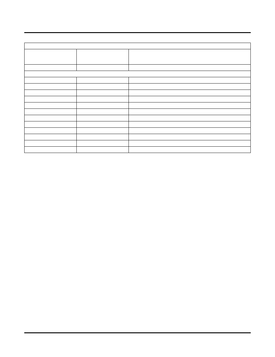
TOH_xx_EN
O
Indicates state of register settings for TOHxx_EN
PROT_SWITCH_AA
I
Parallel protection switch select, Channels AA and AB
PROT_SWITCH_AC
I
Parallel protection switch select, Channels AC and AD
PROT_SWITCH_BA
I
Parallel protection switch select, Channels BA and BB
PROT_SWITCH_BC
I
Parallel protection switch select, Channels BC and BD
LVDS_PROT_AA
I
LVDS protection switch select, Channel AA
LVSD_PROT_AB
I
LVDS protection switch select, Channel AB
LVDS_PROT_AC
I
LVDS protection switch select, Channel AC
LVDS_PROT_AD
I
LVDS protection switch select, Channel AD
LVDS_PROT_BA
I
LVDS protection switch select, Channel BA
LVDS_PROT_BB
I
LVDS protection switch select, Channel BB
LVDS_PROT_BC
I
LVDS protection switch select, Channel BC
LVDS_PROT_BD
I
LVDS protection switch select, Channel BD
Table 15. FPGA/Embedded Core Interface Signals (Continued)
ORT8850 FPGA/Embedded Core Interface Signals - SONET Blocks
FPGA/Embedded Core
Interface Signal Name
xx=[AA,…,BD]
Input (I) to or Output (O)
from Core
Signal Description
相關(guān)PDF資料 |
PDF描述 |
|---|---|
| P1010PSE5HFA | MPU PROTO 800/667 425-TEPBGA1 |
| P1013NXN2LFB | IC MPU 1067MHZ 689TEPBGA |
| P1013PSE2EFA | IC MPU PROTO 600MHZ 689-TEPBGA |
| P1014NSN5DFA | IC MPU 800MHZ 425TEPBGA1 |
| P1014NSN5FFA | IC MPU 800MHZ 425TEPBGA1 |
相關(guān)代理商/技術(shù)參數(shù) |
參數(shù)描述 |
|---|---|
| ORT8850L-3BMN680C | 功能描述:FPGA - 現(xiàn)場(chǎng)可編程門(mén)陣列 4992 LUT 278 I/O RoHS:否 制造商:Altera Corporation 系列:Cyclone V E 柵極數(shù)量: 邏輯塊數(shù)量:943 內(nèi)嵌式塊RAM - EBR:1956 kbit 輸入/輸出端數(shù)量:128 最大工作頻率:800 MHz 工作電源電壓:1.1 V 最大工作溫度:+ 70 C 安裝風(fēng)格:SMD/SMT 封裝 / 箱體:FBGA-256 |
| ORT9303 | 制造商:BOT 制造商全稱(chēng):Bedford Opto Technology Ltd. 功能描述:3 ELEMENT PCB MOUNT 1.8mm LED ARRAY |
| ORT9303B | 制造商:BOT 制造商全稱(chēng):Bedford Opto Technology Ltd. 功能描述:3 ELEMENT PCB MOUNT 1.8mm LED ARRAY |
| ORT9303BL | 制造商:BOT 制造商全稱(chēng):Bedford Opto Technology Ltd. 功能描述:3 ELEMENT PCB MOUNT 1.8mm LED ARRAY |
| ORT9303G | 制造商:BOT 制造商全稱(chēng):Bedford Opto Technology Ltd. 功能描述:3 ELEMENT PCB MOUNT 1.8mm LED ARRAY |
發(fā)布緊急采購(gòu),3分鐘左右您將得到回復(fù)。