- 您現(xiàn)在的位置:買賣IC網 > PDF目錄384032 > TVP3026-175M (Texas Instruments, Inc.) Video Interface PALETTE Exract(組合像素模式視頻接口調色器) PDF資料下載
參數(shù)資料
| 型號: | TVP3026-175M |
| 廠商: | Texas Instruments, Inc. |
| 英文描述: | Video Interface PALETTE Exract(組合像素模式視頻接口調色器) |
| 中文描述: | 視頻接口調色板Exract(組合像素模式視頻接口調色器) |
| 文件頁數(shù): | 57/107頁 |
| 文件大小: | 707K |
| 代理商: | TVP3026-175M |
第1頁第2頁第3頁第4頁第5頁第6頁第7頁第8頁第9頁第10頁第11頁第12頁第13頁第14頁第15頁第16頁第17頁第18頁第19頁第20頁第21頁第22頁第23頁第24頁第25頁第26頁第27頁第28頁第29頁第30頁第31頁第32頁第33頁第34頁第35頁第36頁第37頁第38頁第39頁第40頁第41頁第42頁第43頁第44頁第45頁第46頁第47頁第48頁第49頁第50頁第51頁第52頁第53頁第54頁第55頁第56頁當前第57頁第58頁第59頁第60頁第61頁第62頁第63頁第64頁第65頁第66頁第67頁第68頁第69頁第70頁第71頁第72頁第73頁第74頁第75頁第76頁第77頁第78頁第79頁第80頁第81頁第82頁第83頁第84頁第85頁第86頁第87頁第88頁第89頁第90頁第91頁第92頁第93頁第94頁第95頁第96頁第97頁第98頁第99頁第100頁第101頁第102頁第103頁第104頁第105頁第106頁第107頁
2–43
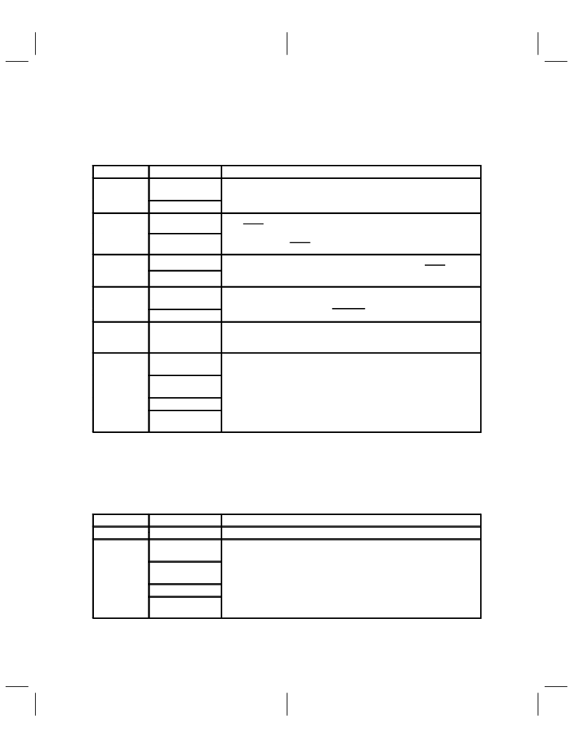
2.15.3
The indirect cursor-control register is accessed using the indirect register map. This register provides for
enabling and disabling the cursor and other cursor controls. The cursor mode-select may also be controlled
using the direct cursor-control register. The indirect cursor-control register definition is listed in Table 2–28.
Table 2–28. Indirect Cursor-Control Register
Indirect Cursor-Control Register (Index: 0x06, Access: R/W, Default: 0x00)
BIT NAME
VALUES
DESCRIPTION
CCR7
0: Use indirect
CCR (default)
Cursor control register select. CCR7 selects which cursor control register is
used (direct or indirect). The video BIOS must initialize this bit to 1 for driver
software that uses the direct cursor control register.
1: Use direct CCR
CCR6
0: Normal (default)
ODD/EVEN sense invert. When CCR6 is reset to 0, the field indicator
ODD/EVEN used by the hardware cursor in interlaced display mode, is set to
1 for the odd field and is reset to 0 for the even field. When CCR6 is set to 1,
the polarity of ODD/EVEN is the opposite.
1: Invert
p y
CCR5
0: Disable (default)
Enable interlaced cursor. When CCR5 is set to 1, interlaced cursor operation
is enabled During interlaced cursor operation the ODD/EVEN terminal
isena bled. During interlaced cursor operation, the ODD/EVEN terminal
indicates the odd or even field, as determined by value in CCR6.
1: Enable
CCR4
0: 2048 pixels
(default)
Vertical blank detection method. Vertical blank is detected using only the blank
signal. The logic detects when there has been either 2048 or 4096 consecutive
dot clocks between rising edges of BLANK.
1: 4096 pixels
CCR3, CCR2
00: (default)
Cursor RAM address bits 9 and 8. CCR3 is bit 9 and CCR2 is bit 8. These bits
are used with the lower 8 bits of the cursor RAM address supplied by the cursor
RAM address register in the direct register map.
CCR1 CCR0
CCR1, CCR0
00: Cursor off
(default)
Cursor mode select. CCR1 and CCR0 disable the cursor and select the format
used to interpret the information stored in the cursor RAM when displaying the
cursor. See Table 2–27.
dCCR0di
h f
p y g
01: Three-color
cursor
10: XGA cursor
11: X-windows
cursor
2.15.4
Direct Cursor-Control Register (Direct Register: 1001, Access: R/W,
Default: 0x00)
The direct cursor control register is accessed using the direct register map. This register provides an
alternate means of enabling and disabling the cursor and selecting the cursor mode. This register is provided
for compatibility with commonly used software drivers. The direct cursor-control register definition is listed
in Table 2–29.
Table 2–29. Direct Cursor-Control Register
BIT NAME
DCC7–DCC2
VALUES
DESCRIPTION
000000
00: Cursor off
(default)
Reserved
DCC1 DCC0
DCC1, DCC0
Cursor mode select. DCC1 and DCC0 disable the cursor and select the format
used to interp
cursor. See Table 2–27.
dDCC0di
h f
p y g
01: Three color
cursor
10: XGA cursor
11: X-windows
cursor
相關PDF資料 |
PDF描述 |
|---|---|
| TVP3026-220 | Video Interface PALETTE Exract(組合像素模式視頻接口調色器) |
| TVP3026-250 | Video Interface PALETTE Exract(組合像素模式視頻接口調色器) |
| TX24 | 60.8 MM 5 X 8 DOT MATRIX DISPLAYS |
| TXB0102DCTR | 2-BIT BIDIRECTIONAL VOLTAGE-LEVEL TRANSLATOR WITH AUTO DIRECTION SENSING AND 【15-kV ESD PROTECTION |
| TXB0102DCTT | 2-BIT BIDIRECTIONAL VOLTAGE-LEVEL TRANSLATOR WITH AUTO DIRECTION SENSING AND 【15-kV ESD PROTECTION |
相關代理商/技術參數(shù) |
參數(shù)描述 |
|---|---|
| TVP3026-175MDN | 制造商:未知廠家 制造商全稱:未知廠家 功能描述:Video DAC with Color Palette (RAMDAC) |
| TVP3026-175MHFG | 制造商:未知廠家 制造商全稱:未知廠家 功能描述:Video DAC with Color Palette (RAMDAC) |
| TVP3026-175MHFGB | 制造商:未知廠家 制造商全稱:未知廠家 功能描述:Video DAC with Color Palette (RAMDAC) |
| TVP3026-175PCE | 制造商:Rochester Electronics LLC 功能描述:- Bulk |
| TVP3026-220AMDN | 制造商:TI 制造商全稱:Texas Instruments 功能描述:Video Interface Palette |
發(fā)布緊急采購,3分鐘左右您將得到回復。