- 您現(xiàn)在的位置:買賣IC網(wǎng) > PDF目錄383724 > ORT82G5 ORCA ORT82G5 1.0.1-25/2.0-2.5/3.125 Gbits/s Backplane Interface FPSC PDF資料下載
參數(shù)資料
| 型號(hào): | ORT82G5 |
| 英文描述: | ORCA ORT82G5 1.0.1-25/2.0-2.5/3.125 Gbits/s Backplane Interface FPSC |
| 中文描述: | ORCA的ORT82G5 1.0.1-25/2.0-2.5/3.125 Gb /秒背板接口促進(jìn)文化基金 |
| 文件頁(yè)數(shù): | 55/92頁(yè) |
| 文件大小: | 1823K |
| 代理商: | ORT82G5 |
第1頁(yè)第2頁(yè)第3頁(yè)第4頁(yè)第5頁(yè)第6頁(yè)第7頁(yè)第8頁(yè)第9頁(yè)第10頁(yè)第11頁(yè)第12頁(yè)第13頁(yè)第14頁(yè)第15頁(yè)第16頁(yè)第17頁(yè)第18頁(yè)第19頁(yè)第20頁(yè)第21頁(yè)第22頁(yè)第23頁(yè)第24頁(yè)第25頁(yè)第26頁(yè)第27頁(yè)第28頁(yè)第29頁(yè)第30頁(yè)第31頁(yè)第32頁(yè)第33頁(yè)第34頁(yè)第35頁(yè)第36頁(yè)第37頁(yè)第38頁(yè)第39頁(yè)第40頁(yè)第41頁(yè)第42頁(yè)第43頁(yè)第44頁(yè)第45頁(yè)第46頁(yè)第47頁(yè)第48頁(yè)第49頁(yè)第50頁(yè)第51頁(yè)第52頁(yè)第53頁(yè)第54頁(yè)當(dāng)前第55頁(yè)第56頁(yè)第57頁(yè)第58頁(yè)第59頁(yè)第60頁(yè)第61頁(yè)第62頁(yè)第63頁(yè)第64頁(yè)第65頁(yè)第66頁(yè)第67頁(yè)第68頁(yè)第69頁(yè)第70頁(yè)第71頁(yè)第72頁(yè)第73頁(yè)第74頁(yè)第75頁(yè)第76頁(yè)第77頁(yè)第78頁(yè)第79頁(yè)第80頁(yè)第81頁(yè)第82頁(yè)第83頁(yè)第84頁(yè)第85頁(yè)第86頁(yè)第87頁(yè)第88頁(yè)第89頁(yè)第90頁(yè)第91頁(yè)第92頁(yè)
Agere Systems Inc.
55
Preliminary Data Sheet
July 2001
1.0-1.25/2.0-2.5/3.125 Gbits/s Backplane Interface
ORCA
ORT82G5 FPSC Eight-Channel
HSI Electrical and Timing Characteristics
(continued)
2391(F)
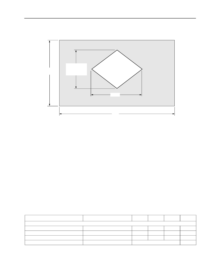
Figure 19. Receive Data Eye-diagram Template (Differential)
Figure 19 provides a graphical characterization of the SERDES receiver input requirements. It provides guidance
on a number of input parameters, including signal amplitude and rise time lints, noise and jitter limits, and P and N
input skew tolerance. it is believed that incoming data patterns falling within the shaded region of the template will
be received without error (BER < 10E-12).
Data pattern eye-opening at the receive end of a link is considered the ultimate measures of received signal qual-
ity. Almost all detrimental characteristics of transmit signal and the interconnection link design result in eye-closure.
This combined with the eye-opening limitations of the line receiver can provide a good indication of a links ability to
transfer data error-free.
Signal jitter is of special interest to system designers. It is often the primary limiting characteristic of long digital
links and of systems with high noise level environments. An interesting characteristic of the clock and data recov-
ery (CDR) portion of the ORT82G5 SERDES receiver is its ability to filter incoming signal jitter that is below the
clock recover bandwidth (estimated to be about 3 MHz). For signals with high levels of low frequency jitter the
receiver can detect incoming data, error-free, with eye-openings significantly less than that of Figure 19. This phe-
nomena has been observed in the laboratory.
Eye-diagram measurement and simulation are excellent tools of design. They are both highly recommended when
designing serial link interconnections and evaluating signal integrity.
Table 17. Receiver Specifications
Parameter
Conditions
Min
Typ
Max
Unit
Input Data
Stream of Nontransitions
Phase change, Input Signal
Eye Opening
Jitter Tolerance
—
—
—
—
—
—
0.4
—
—
—
60
TBD
—
bits
ps
U
IP-P
U
IP-P
TBD
0.4UI
200 mV @
1.0
—
2.5 GBits/s,
350 mV @
3.125 GBits/s
1.2 V
UI
相關(guān)PDF資料 |
PDF描述 |
|---|---|
| ORT8850 | Field-Programmable System Chip (FPSC) Eight-Channel x 850 Mbits/s Backplane Transceiver |
| ORT8850H | Field-Programmable System Chip (FPSC) Eight-Channel x 850 Mbits/s Backplane Transceiver |
| ORT8850L | Field-Programmable System Chip (FPSC) Eight-Channel x 850 Mbits/s Backplane Transceiver |
| OS1001 | Interface IC |
| OS1010 | Optoelectronic |
相關(guān)代理商/技術(shù)參數(shù) |
參數(shù)描述 |
|---|---|
| ORT82G5-1BM680C | 功能描述:FPGA - 現(xiàn)場(chǎng)可編程門陣列 10368 LUT 372 I/O RoHS:否 制造商:Altera Corporation 系列:Cyclone V E 柵極數(shù)量: 邏輯塊數(shù)量:943 內(nèi)嵌式塊RAM - EBR:1956 kbit 輸入/輸出端數(shù)量:128 最大工作頻率:800 MHz 工作電源電壓:1.1 V 最大工作溫度:+ 70 C 安裝風(fēng)格:SMD/SMT 封裝 / 箱體:FBGA-256 |
| ORT82G5-1BM680I | 功能描述:FPGA - 現(xiàn)場(chǎng)可編程門陣列 10368 LUT 372 I/O RoHS:否 制造商:Altera Corporation 系列:Cyclone V E 柵極數(shù)量: 邏輯塊數(shù)量:943 內(nèi)嵌式塊RAM - EBR:1956 kbit 輸入/輸出端數(shù)量:128 最大工作頻率:800 MHz 工作電源電壓:1.1 V 最大工作溫度:+ 70 C 安裝風(fēng)格:SMD/SMT 封裝 / 箱體:FBGA-256 |
| ORT82G5-1F680C | 功能描述:FPGA - 現(xiàn)場(chǎng)可編程門陣列 ORCA FPSC 3.7GBITS/s BP XCVR 643K RoHS:否 制造商:Altera Corporation 系列:Cyclone V E 柵極數(shù)量: 邏輯塊數(shù)量:943 內(nèi)嵌式塊RAM - EBR:1956 kbit 輸入/輸出端數(shù)量:128 最大工作頻率:800 MHz 工作電源電壓:1.1 V 最大工作溫度:+ 70 C 安裝風(fēng)格:SMD/SMT 封裝 / 箱體:FBGA-256 |
| ORT82G5-1F680I | 功能描述:FPGA - 現(xiàn)場(chǎng)可編程門陣列 ORCA FPSC 2.7Gbits/s BP XCVR 643K RoHS:否 制造商:Altera Corporation 系列:Cyclone V E 柵極數(shù)量: 邏輯塊數(shù)量:943 內(nèi)嵌式塊RAM - EBR:1956 kbit 輸入/輸出端數(shù)量:128 最大工作頻率:800 MHz 工作電源電壓:1.1 V 最大工作溫度:+ 70 C 安裝風(fēng)格:SMD/SMT 封裝 / 箱體:FBGA-256 |
| ORT82G5-1FN680C | 功能描述:FPGA - 現(xiàn)場(chǎng)可編程門陣列 ORCA FPSC 1.5V 3.7 G b Bpln Xcvr 643K Gt RoHS:否 制造商:Altera Corporation 系列:Cyclone V E 柵極數(shù)量: 邏輯塊數(shù)量:943 內(nèi)嵌式塊RAM - EBR:1956 kbit 輸入/輸出端數(shù)量:128 最大工作頻率:800 MHz 工作電源電壓:1.1 V 最大工作溫度:+ 70 C 安裝風(fēng)格:SMD/SMT 封裝 / 箱體:FBGA-256 |
發(fā)布緊急采購(gòu),3分鐘左右您將得到回復(fù)。