- 您現(xiàn)在的位置:買賣IC網(wǎng) > PDF目錄383724 > ORT82G5 ORCA ORT82G5 1.0.1-25/2.0-2.5/3.125 Gbits/s Backplane Interface FPSC PDF資料下載
參數(shù)資料
| 型號: | ORT82G5 |
| 英文描述: | ORCA ORT82G5 1.0.1-25/2.0-2.5/3.125 Gbits/s Backplane Interface FPSC |
| 中文描述: | ORCA的ORT82G5 1.0.1-25/2.0-2.5/3.125 Gb /秒背板接口促進文化基金 |
| 文件頁數(shù): | 44/92頁 |
| 文件大?。?/td> | 1823K |
| 代理商: | ORT82G5 |
第1頁第2頁第3頁第4頁第5頁第6頁第7頁第8頁第9頁第10頁第11頁第12頁第13頁第14頁第15頁第16頁第17頁第18頁第19頁第20頁第21頁第22頁第23頁第24頁第25頁第26頁第27頁第28頁第29頁第30頁第31頁第32頁第33頁第34頁第35頁第36頁第37頁第38頁第39頁第40頁第41頁第42頁第43頁當前第44頁第45頁第46頁第47頁第48頁第49頁第50頁第51頁第52頁第53頁第54頁第55頁第56頁第57頁第58頁第59頁第60頁第61頁第62頁第63頁第64頁第65頁第66頁第67頁第68頁第69頁第70頁第71頁第72頁第73頁第74頁第75頁第76頁第77頁第78頁第79頁第80頁第81頁第82頁第83頁第84頁第85頁第86頁第87頁第88頁第89頁第90頁第91頁第92頁
44
Agere Systems Inc.
Preliminary Data Sheet
July 2001
1.0-1.25/2.0-2.5/3.125 Gbits/s Backplane Interface
ORCA
ORT82G5 FPSC Eight-Channel
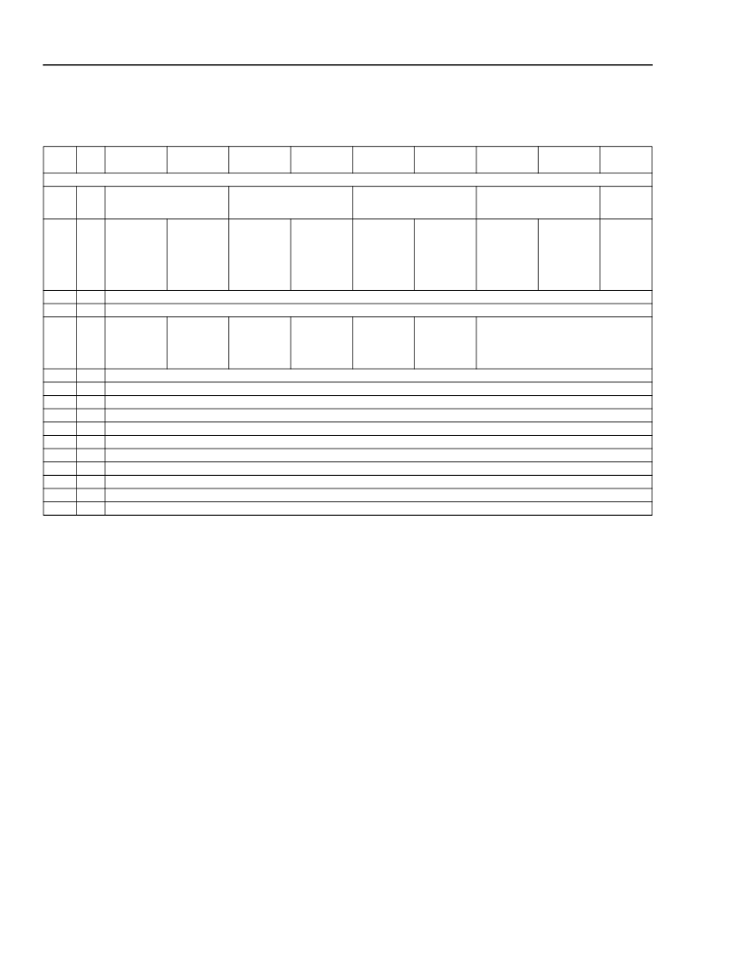
Memory Map
(continued)
Table 12. Memory Map
(continued)
* For XAUISTAT_Ay (address 0x30804), the definitions of these bits are:
00—No synchronization.
01—Synchronization done.
10—Synchronization done no comma has been detected.
11—Not used.
Addr
(Hex)
Status Registers A
30804
A16
Reg
#
DB0
DB1
DB2
DB3
DB4
DB5
DB6
DB7
Default
Value
XAUISTAT_AA*
Status of XAUI link state
machine for bank A, channel A
DEMUXWAS_
AA
Status of
deMUX word
alignment for
bank A, chan-
nel A
XAUISTAT_AB*
Status of XAUI link state
machine for bank A, channel B
DEMUXWAS_
AC
Status of
deMUX word
alignment for
bank A, chan-
nel C
XAUISTAT_AC*
Status of XAUI link state
machine for bank A, channel C
CH248_SYNC
_AA
Alignment
completed for
AA
XAUISTAT_AD*
Status of XAUI link state
machine for bank A, channel D
CH248_SYNC
_AC
Alignment
completed for
AC
00
30805
A17
DEMUXWAS_
AB
Status of
deMUX word
alignment for
bank A, chan-
nel B
DEMUXWAS
_AD
Status of
deMUX word
alignment for
bank A, chan-
nel D
CH248_SYNC
_AB
Alignment
completed for
AB
CH248_SYNC
_AD
Alignment
completed for
AD
00
30806
30807
30814
A18
A19
A20
Reserved for future use
Reserved for future use
SYNC2_A1
OOS
Alignment out
of sync for AA
and AB
and AD
Reserved for future use
Reserved for future use
Reserved for future use
Reserved for future use
Reserved for future use
Reserved for future use
Reserved for future use
Reserved for future use
Reserved for future use
Reserved for future use
Reserved for future use
SYNC2_A1
OVFL
Alignment
FIFO overflow
AA and AB
SYNC2_A2
OVFL
Alignment
FIFO overflow
AC and AD
SYNC4_A
OVFL
Alignment
FIFO overflow
for A[A:D]
SYNC2_A2
OOS
Alignment out
of sync for AC
SYNC4_A_O
OS
Alignment out
of sync for
A[A:D]
Reserved for future use
30815
30816
30817
30824
30825
30826
30827
30834
30835
30836
30837
A21
A22
A23
A24
A25
A26
A27
A28
A29
A30
A31
相關(guān)PDF資料 |
PDF描述 |
|---|---|
| ORT8850 | Field-Programmable System Chip (FPSC) Eight-Channel x 850 Mbits/s Backplane Transceiver |
| ORT8850H | Field-Programmable System Chip (FPSC) Eight-Channel x 850 Mbits/s Backplane Transceiver |
| ORT8850L | Field-Programmable System Chip (FPSC) Eight-Channel x 850 Mbits/s Backplane Transceiver |
| OS1001 | Interface IC |
| OS1010 | Optoelectronic |
相關(guān)代理商/技術(shù)參數(shù) |
參數(shù)描述 |
|---|---|
| ORT82G5-1BM680C | 功能描述:FPGA - 現(xiàn)場可編程門陣列 10368 LUT 372 I/O RoHS:否 制造商:Altera Corporation 系列:Cyclone V E 柵極數(shù)量: 邏輯塊數(shù)量:943 內(nèi)嵌式塊RAM - EBR:1956 kbit 輸入/輸出端數(shù)量:128 最大工作頻率:800 MHz 工作電源電壓:1.1 V 最大工作溫度:+ 70 C 安裝風格:SMD/SMT 封裝 / 箱體:FBGA-256 |
| ORT82G5-1BM680I | 功能描述:FPGA - 現(xiàn)場可編程門陣列 10368 LUT 372 I/O RoHS:否 制造商:Altera Corporation 系列:Cyclone V E 柵極數(shù)量: 邏輯塊數(shù)量:943 內(nèi)嵌式塊RAM - EBR:1956 kbit 輸入/輸出端數(shù)量:128 最大工作頻率:800 MHz 工作電源電壓:1.1 V 最大工作溫度:+ 70 C 安裝風格:SMD/SMT 封裝 / 箱體:FBGA-256 |
| ORT82G5-1F680C | 功能描述:FPGA - 現(xiàn)場可編程門陣列 ORCA FPSC 3.7GBITS/s BP XCVR 643K RoHS:否 制造商:Altera Corporation 系列:Cyclone V E 柵極數(shù)量: 邏輯塊數(shù)量:943 內(nèi)嵌式塊RAM - EBR:1956 kbit 輸入/輸出端數(shù)量:128 最大工作頻率:800 MHz 工作電源電壓:1.1 V 最大工作溫度:+ 70 C 安裝風格:SMD/SMT 封裝 / 箱體:FBGA-256 |
| ORT82G5-1F680I | 功能描述:FPGA - 現(xiàn)場可編程門陣列 ORCA FPSC 2.7Gbits/s BP XCVR 643K RoHS:否 制造商:Altera Corporation 系列:Cyclone V E 柵極數(shù)量: 邏輯塊數(shù)量:943 內(nèi)嵌式塊RAM - EBR:1956 kbit 輸入/輸出端數(shù)量:128 最大工作頻率:800 MHz 工作電源電壓:1.1 V 最大工作溫度:+ 70 C 安裝風格:SMD/SMT 封裝 / 箱體:FBGA-256 |
| ORT82G5-1FN680C | 功能描述:FPGA - 現(xiàn)場可編程門陣列 ORCA FPSC 1.5V 3.7 G b Bpln Xcvr 643K Gt RoHS:否 制造商:Altera Corporation 系列:Cyclone V E 柵極數(shù)量: 邏輯塊數(shù)量:943 內(nèi)嵌式塊RAM - EBR:1956 kbit 輸入/輸出端數(shù)量:128 最大工作頻率:800 MHz 工作電源電壓:1.1 V 最大工作溫度:+ 70 C 安裝風格:SMD/SMT 封裝 / 箱體:FBGA-256 |
發(fā)布緊急采購,3分鐘左右您將得到回復。