- 您現(xiàn)在的位置:買賣IC網(wǎng) > PDF目錄371670 > 83C795 (SMSC Corporation) Ethernet System Controller PDF資料下載
參數(shù)資料
| 型號(hào): | 83C795 |
| 廠商: | SMSC Corporation |
| 英文描述: | Ethernet System Controller |
| 中文描述: | 以太網(wǎng)系統(tǒng)控制器 |
| 文件頁(yè)數(shù): | 58/136頁(yè) |
| 文件大小: | 1996K |
| 代理商: | 83C795 |
第1頁(yè)第2頁(yè)第3頁(yè)第4頁(yè)第5頁(yè)第6頁(yè)第7頁(yè)第8頁(yè)第9頁(yè)第10頁(yè)第11頁(yè)第12頁(yè)第13頁(yè)第14頁(yè)第15頁(yè)第16頁(yè)第17頁(yè)第18頁(yè)第19頁(yè)第20頁(yè)第21頁(yè)第22頁(yè)第23頁(yè)第24頁(yè)第25頁(yè)第26頁(yè)第27頁(yè)第28頁(yè)第29頁(yè)第30頁(yè)第31頁(yè)第32頁(yè)第33頁(yè)第34頁(yè)第35頁(yè)第36頁(yè)第37頁(yè)第38頁(yè)第39頁(yè)第40頁(yè)第41頁(yè)第42頁(yè)第43頁(yè)第44頁(yè)第45頁(yè)第46頁(yè)第47頁(yè)第48頁(yè)第49頁(yè)第50頁(yè)第51頁(yè)第52頁(yè)第53頁(yè)第54頁(yè)第55頁(yè)第56頁(yè)第57頁(yè)當(dāng)前第58頁(yè)第59頁(yè)第60頁(yè)第61頁(yè)第62頁(yè)第63頁(yè)第64頁(yè)第65頁(yè)第66頁(yè)第67頁(yè)第68頁(yè)第69頁(yè)第70頁(yè)第71頁(yè)第72頁(yè)第73頁(yè)第74頁(yè)第75頁(yè)第76頁(yè)第77頁(yè)第78頁(yè)第79頁(yè)第80頁(yè)第81頁(yè)第82頁(yè)第83頁(yè)第84頁(yè)第85頁(yè)第86頁(yè)第87頁(yè)第88頁(yè)第89頁(yè)第90頁(yè)第91頁(yè)第92頁(yè)第93頁(yè)第94頁(yè)第95頁(yè)第96頁(yè)第97頁(yè)第98頁(yè)第99頁(yè)第100頁(yè)第101頁(yè)第102頁(yè)第103頁(yè)第104頁(yè)第105頁(yè)第106頁(yè)第107頁(yè)第108頁(yè)第109頁(yè)第110頁(yè)第111頁(yè)第112頁(yè)第113頁(yè)第114頁(yè)第115頁(yè)第116頁(yè)第117頁(yè)第118頁(yè)第119頁(yè)第120頁(yè)第121頁(yè)第122頁(yè)第123頁(yè)第124頁(yè)第125頁(yè)第126頁(yè)第127頁(yè)第128頁(yè)第129頁(yè)第130頁(yè)第131頁(yè)第132頁(yè)第133頁(yè)第134頁(yè)第135頁(yè)第136頁(yè)
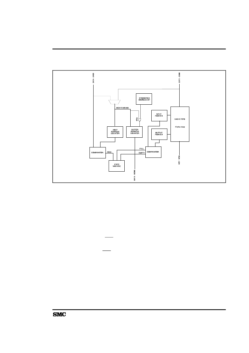
6.1.1
The Zero Wait State signal tells the microprocessor
that it can complete the present bus cycle without
inserting any additional wait cycles. For 16-bit
memory access, this means zero wait states are
inserted by the host bus logic and the access cycle
completes in 2 bus clocks. When asserted for an 8
bit memory access, an ISA bus automatically
inserts the minimum of 2 wait states.
Zero Wait State Response to Host
The response algorithm for the ZWS line depends
upon the memory width, the host access type and
whether the board has been enabled to act as a
16-bit device. The appropriate ZWS response logic
is selected on the basis of the BPR.M16EN control
bit and whether the board is in an 8- or 16-bit slot.
The memory cache can accommodate zero wait
state timing if the following conditions are met:
1. The type of host access matches the current
mode of the cache,
2. The host address matches the value in the
host counter, and
3. The cache either contains at least one valid
data word for reads or has room for at least
one more word for writes.
For writes, zero wait states are also always possible
if the cache is in read mode, or if it is currently
empty.
There is a Zero Wait Enable bit in one of the host
interface registers (CR.ZWSEN) which can be used
to prevent the 83C795 from asserting the Zero Wait
State signal.
6.1.2
Staggered address transfers occur when the host
attempts 16-bit data transfers from system memory
to the local buffer RAM and finds that the address
of the system data differs from the local address in
the least significant bit (one is even, one is odd). In
consequence, the ISA bus forbids 16-bit accesses
to odd locations and breaks the transfer into two
8-bit cycles which run considerably slower.
Staggered Address Transfers
To overcome this on the 795:
FIGURE 6-1. MEMORY CACHE ARRANGEMENT
HOST INTERFACE SECTION
83C795
45
相關(guān)PDF資料 |
PDF描述 |
|---|---|
| 84063 | The Constituents of Semiconductor Components |
| 8406601QA | CMOS Programmable Peripheral Interface |
| 8406601XA | CMOS Programmable Peripheral Interface |
| 8406602XA | CMOS Programmable Peripheral Interface |
| 8406602QA | CMOS Programmable Peripheral Interface |
相關(guān)代理商/技術(shù)參數(shù) |
參數(shù)描述 |
|---|---|
| 83C800-009 | 制造商:DRS 功能描述: |
| 83C825EQFP | 制造商:SMSC 功能描述: |
| 83C845 | 制造商:PHILIPS 制造商全稱:NXP Semiconductors 功能描述:Microcontrollers for TV and video MTV |
| 83C851 | 制造商:PHILIPS 制造商全稱:NXP Semiconductors 功能描述:CMOS single-chip 8-bit microcontroller with on-chip EEPROM |
| 83C852DIE | 制造商:未知廠家 制造商全稱:未知廠家 功能描述:8-Bit Microcontroller |
發(fā)布緊急采購(gòu),3分鐘左右您將得到回復(fù)。