- 您現(xiàn)在的位置:買賣IC網(wǎng) > PDF目錄371436 > 28F640C3 (Intel Corp.) 3 Volt Advanced Boot Block Flash Memory(3 V 高級快速引導(dǎo)塊閃速存儲器) PDF資料下載
參數(shù)資料
| 型號: | 28F640C3 |
| 廠商: | Intel Corp. |
| 英文描述: | 3 Volt Advanced Boot Block Flash Memory(3 V 高級快速引導(dǎo)塊閃速存儲器) |
| 中文描述: | 3伏高級啟動塊閃存(3伏高級快速引導(dǎo)塊閃速存儲器) |
| 文件頁數(shù): | 14/70頁 |
| 文件大?。?/td> | 894K |
| 代理商: | 28F640C3 |
第1頁第2頁第3頁第4頁第5頁第6頁第7頁第8頁第9頁第10頁第11頁第12頁第13頁當(dāng)前第14頁第15頁第16頁第17頁第18頁第19頁第20頁第21頁第22頁第23頁第24頁第25頁第26頁第27頁第28頁第29頁第30頁第31頁第32頁第33頁第34頁第35頁第36頁第37頁第38頁第39頁第40頁第41頁第42頁第43頁第44頁第45頁第46頁第47頁第48頁第49頁第50頁第51頁第52頁第53頁第54頁第55頁第56頁第57頁第58頁第59頁第60頁第61頁第62頁第63頁第64頁第65頁第66頁第67頁第68頁第69頁第70頁
28F800C3, 28F160C3, 28F320C3, 28F640C3
8
3UHOLPLQDU\
3.1.2
Output Disable
With OE# at a logic
-
high level (V
IH
), the device outputs are disabled. Output pins are placed in a
high
-
impedance state.
3.1.3
Standby
Deselecting the device by bringing CE# to a logic
-
high level (V
IH
) places the device in standby
mode, which substantially reduces device power consumption without any latency for subsequent
read accesses. In standby, outputs are placed in a high-impedance state independent of OE#. If
deselected during program or erase operation, the device continues to consume active power until
the program or erase operation is complete.
NOTES:
1. X must be V
, V
for control pins and addresses.
2. See DC Characteristicsfor V
, V
, V
, V
, voltages.
3. Manufacturer and device codes may also be accessed in read configuration mode (A
1–
A
20
= 0). See
Table 4
on page 10
.
4. To program or erase the lockable blocks, hold WP# at V
.
5. Refer to
Table 5 on page 13
for valid D
during a write operation.
6. RP# must be at GND
±
0.2 V to meet the maximum deep power-down current specified.
8-bit devices use only DQ [0:7], 16-bit devices use DQ [0:15].
3.1.4
Reset
From read mode, RP# at V
IL
for time t
PLPH
deselects the memory, places output drivers in a high
-
impedance state, and turns off all internal circuits. After return from reset, a time t
PHQV
is required
until the initial read access outputs are valid. A delay (t
PHWL
or t
PHEL
) is required after return from
reset before a write can be initiated. After this wake
-
up interval, normal operation is restored. The
CUI resets to read array mode, the status register is set to 80H, and all blocks are locked. This case
is shown in
Figure 10, “AC Waveform: Reset Operations” on page 39
(section A).
If RP# is taken low for time t
PLPH
during a program or erase operation, the operation will be
aborted and the memory contents at the aborted location (for a program) or block (for an erase) are
no longer valid, since the data may be partially erased or written. The abort process goes through
the following sequence: When RP# goes low, the device shuts down the operation in progress, a
process which takes time t
PLRH
to complete. After this time t
PLRH
, the part will either reset to read
array mode (if RP# has gone high during t
PLRH
,
Figure 10
, section B) or enter reset mode (if RP# is
still logic low after t
PLRH
,
Figure 10
, section C). In both cases, after returning from an aborted
operation, the relevant time t
PHQV
or t
PHWL
/t
PHEL
must be observed before a read or write
operation is initiated, as discussed in the previous paragraph. However, in this case, these delays
are referenced to the end of t
PLRH
rather than when RP# goes high.
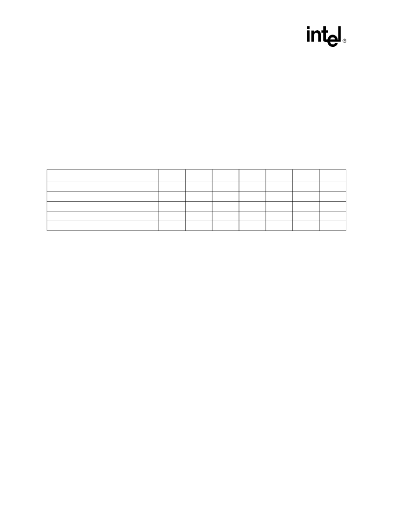
Table 3. Bus Operations
Mode
Notes
RP#
CE#
OE#
WE#
DQ
0–7
DQ
8–15
Read (Array, Status, Configuration, or Query)
1, 2,3
V
IH
V
IL
V
IL
V
IH
D
OUT
D
OUT
Output Disable
1
V
IH
V
IL
V
IH
V
IH
High Z
High Z
Standby
1
V
IH
V
IH
X
X
High Z
High Z
Reset
1,4
V
IL
X
X
X
High Z
High Z
Write
1,4,5,6
V
IH
V
IL
V
IH
V
IL
D
IN
D
IN
相關(guān)PDF資料 |
PDF描述 |
|---|---|
| 28F640J3C-120 | Intel StrataFlash Memory (J3) |
| 28LV64A | 64K (8K x 8) Low Voltage CMOS EEPROM(低壓,64K位, CMOS 并行EEPROM) |
| 28M0U | 60V 300mA MONOLITHIC DIODE ARRAY |
| 28M0DC | 60V 300mA MONOLITHIC DIODE ARRAY |
| 28M0DS | 60V 300mA MONOLITHIC DIODE ARRAY |
相關(guān)代理商/技術(shù)參數(shù) |
參數(shù)描述 |
|---|---|
| 28F640C3BC80 | 制造商: 功能描述: 制造商:undefined 功能描述: |
| 28F640J3C120 | 制造商: 功能描述: 制造商:undefined 功能描述: |
| 28F640J3C-120 | 制造商: 功能描述: 制造商:undefined 功能描述: |
| 28F640J3D75 | 制造商:Intel 功能描述: 制造商: 功能描述: 制造商:undefined 功能描述: |
| 28F640J5 | 制造商:INTEL 制造商全稱:Intel Corporation 功能描述:5 Volt Intel StrataFlash? Memory |
發(fā)布緊急采購,3分鐘左右您將得到回復(fù)。