- 您現(xiàn)在的位置:買賣IC網(wǎng) > PDF目錄372961 > Z85233 (ZiLOG, Inc.) The Zilog SCC Serial Communication Controller PDF資料下載
參數(shù)資料
| 型號: | Z85233 |
| 廠商: | ZiLOG, Inc. |
| 英文描述: | The Zilog SCC Serial Communication Controller |
| 中文描述: | Zilog公司鱗癌的串行通信控制器 |
| 文件頁數(shù): | 164/317頁 |
| 文件大小: | 3201K |
| 代理商: | Z85233 |
第1頁第2頁第3頁第4頁第5頁第6頁第7頁第8頁第9頁第10頁第11頁第12頁第13頁第14頁第15頁第16頁第17頁第18頁第19頁第20頁第21頁第22頁第23頁第24頁第25頁第26頁第27頁第28頁第29頁第30頁第31頁第32頁第33頁第34頁第35頁第36頁第37頁第38頁第39頁第40頁第41頁第42頁第43頁第44頁第45頁第46頁第47頁第48頁第49頁第50頁第51頁第52頁第53頁第54頁第55頁第56頁第57頁第58頁第59頁第60頁第61頁第62頁第63頁第64頁第65頁第66頁第67頁第68頁第69頁第70頁第71頁第72頁第73頁第74頁第75頁第76頁第77頁第78頁第79頁第80頁第81頁第82頁第83頁第84頁第85頁第86頁第87頁第88頁第89頁第90頁第91頁第92頁第93頁第94頁第95頁第96頁第97頁第98頁第99頁第100頁第101頁第102頁第103頁第104頁第105頁第106頁第107頁第108頁第109頁第110頁第111頁第112頁第113頁第114頁第115頁第116頁第117頁第118頁第119頁第120頁第121頁第122頁第123頁第124頁第125頁第126頁第127頁第128頁第129頁第130頁第131頁第132頁第133頁第134頁第135頁第136頁第137頁第138頁第139頁第140頁第141頁第142頁第143頁第144頁第145頁第146頁第147頁第148頁第149頁第150頁第151頁第152頁第153頁第154頁第155頁第156頁第157頁第158頁第159頁第160頁第161頁第162頁第163頁當(dāng)前第164頁第165頁第166頁第167頁第168頁第169頁第170頁第171頁第172頁第173頁第174頁第175頁第176頁第177頁第178頁第179頁第180頁第181頁第182頁第183頁第184頁第185頁第186頁第187頁第188頁第189頁第190頁第191頁第192頁第193頁第194頁第195頁第196頁第197頁第198頁第199頁第200頁第201頁第202頁第203頁第204頁第205頁第206頁第207頁第208頁第209頁第210頁第211頁第212頁第213頁第214頁第215頁第216頁第217頁第218頁第219頁第220頁第221頁第222頁第223頁第224頁第225頁第226頁第227頁第228頁第229頁第230頁第231頁第232頁第233頁第234頁第235頁第236頁第237頁第238頁第239頁第240頁第241頁第242頁第243頁第244頁第245頁第246頁第247頁第248頁第249頁第250頁第251頁第252頁第253頁第254頁第255頁第256頁第257頁第258頁第259頁第260頁第261頁第262頁第263頁第264頁第265頁第266頁第267頁第268頁第269頁第270頁第271頁第272頁第273頁第274頁第275頁第276頁第277頁第278頁第279頁第280頁第281頁第282頁第283頁第284頁第285頁第286頁第287頁第288頁第289頁第290頁第291頁第292頁第293頁第294頁第295頁第296頁第297頁第298頁第299頁第300頁第301頁第302頁第303頁第304頁第305頁第306頁第307頁第308頁第309頁第310頁第311頁第312頁第313頁第314頁第315頁第316頁第317頁
Application Note
The Z180 Interfaced with the SCC at MHZ
6-29
7
inserting wait states. With this scheme, you can get the
highest performance with moderate cost.
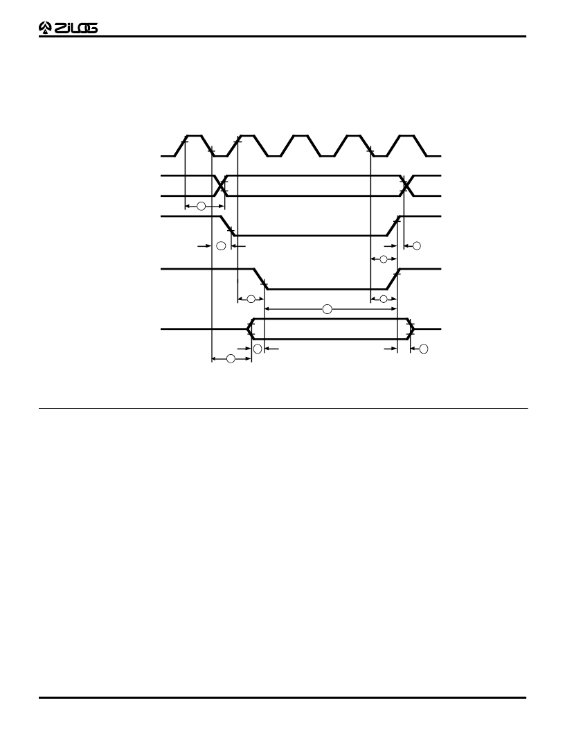
SRAM Write Cycle.
the Z180 write data is stable before the falling edge of /WR
During a Z180 memory write cycle,
(Z180 parameter #24; 15 ns min at 10 MHz). It is stable
throughout the write cycle (Z180 parameter #27; 10 ns min
at 10 MHz). Further, the address is fixed before the falling
edge of /WR. As long as the /WR pulse width meets the
SRAM’s spec, there is no problem (reference Table 2).
Memory Interface Logic
The memory devices (EPROM and SRAM) for this design
are 256K bit (32K byte). There are two possible memory
interface designs:
Connect Address Decode output to /E input. Put the
signal generated by /RD and /MREQ ANDed together to
/OE of EPROM and SRAM. Put the signal generated by
/WR and /MREQ ANDed together to the /WE pin of
SRAM (Figure 4a).
Connect the signal Address ANDed together with inactive
/IORQ to the /E input. Connect /RD to /OE of EPROM and
SRAM, and /WR to /WE pin of SRAM (Figure 4b).
Using the second method, there could be a narrow glitch
on the signal to the /E-pin during I/O cycles and the
Interrupt acknowledge cycle. During I/O cycles, /IORQ and
/RD or /WR go active at almost the same time. Since the
delay times of these signals are similar there is no
“overlapping time” between /CE generated by the address
(/IORQ inactive), and /WR or /RD active. During the
Interrupt Acknowledge cycle, /WR and /RD signals are
inactive.
To keep the design simple and flexible, use the second
method (Figure 4b). To expand memory, decode the
address A15 NANDed with /USRRAM//USRROM and
/IORQ to produce /CSRAM or /CSROM. These are chip
select inputs to chips 55257 or 27C256, respectively. This
either disables or enables on-board ROM or RAM
depending upon selection control.
The circuit on Figure 4b gives the physical memory
address as shown on Figure 5.
If there are no Z80 peripherals and /M1 is enabled (M1E
bit in Z180 OMCR register set to 1), active wait states
occur only during opcode fetch cycles (Figure 6). If the
M1E bit is cleared to 0, /M1E is active only during the
Interrupt Acknowledge cycle and Return from Interrupt
cycle. This case depends on the propagation delay of the
address decoder which uses 135 ns or faster EPROM
assess time (assume there is 20 ns propagation delay).
Figure 6 shows the example of this implementation.
Figure 3. Z180 Memory Write Cycle Timing (One Wait State)
6
22
12
11
26
25
27
Address
/MREQ
/WR
Data
T1
T2
Tw
T3
T1
8
24
23
UM010901-0601
相關(guān)PDF資料 |
PDF描述 |
|---|---|
| Z8602 | CAP 0.033UF 100V 10% X7R AXIAL TR-14 |
| Z860201PSC | 8-BIT MICROCONTROLLER |
| Z860202PSC | Leaded Cartridge Fuse; Current Rating:600mA; Voltage Rating:250V; Fuse Terminals:Axial Lead; Fuse Type:Time Delay; Voltage Rating:250V; Body Material:Glass; Diameter:4.7mm; Fuse Size/Group:5 x 15 mm; Leaded Process Compatible:Yes RoHS Compliant: Yes |
| Z860203PSC | 8-BIT MICROCONTROLLER |
| Z86116 | CAP 0.033UF 100V 10% X7R AXIAL TR-14 |
相關(guān)代理商/技術(shù)參數(shù) |
參數(shù)描述 |
|---|---|
| Z8523310ASG | 功能描述:網(wǎng)絡(luò)控制器與處理器 IC 10 MHZ CMOS ESCC/2 RoHS:否 制造商:Micrel 產(chǎn)品:Controller Area Network (CAN) 收發(fā)器數(shù)量: 數(shù)據(jù)速率: 電源電流(最大值):595 mA 最大工作溫度:+ 85 C 安裝風(fēng)格:SMD/SMT 封裝 / 箱體:PBGA-400 封裝:Tray |
| Z8523310FSC | 功能描述:網(wǎng)絡(luò)控制器與處理器 IC 10MHz CMOS ESCC/2 RoHS:否 制造商:Micrel 產(chǎn)品:Controller Area Network (CAN) 收發(fā)器數(shù)量: 數(shù)據(jù)速率: 電源電流(最大值):595 mA 最大工作溫度:+ 85 C 安裝風(fēng)格:SMD/SMT 封裝 / 箱體:PBGA-400 封裝:Tray |
| Z8523310FSC00TR | 功能描述:IC ESCC 44QFP RoHS:否 類別:集成電路 (IC) >> 接口 - 控制器 系列:EMSCC™ 標(biāo)準(zhǔn)包裝:4,900 系列:- 控制器類型:USB 2.0 控制器 接口:串行 電源電壓:3 V ~ 3.6 V 電流 - 電源:135mA 工作溫度:0°C ~ 70°C 安裝類型:表面貼裝 封裝/外殼:36-VFQFN 裸露焊盤 供應(yīng)商設(shè)備封裝:36-QFN(6x6) 包裝:* 其它名稱:Q6396337A |
| Z8523310FSG | 功能描述:網(wǎng)絡(luò)控制器與處理器 IC 10MHz CMOS ESCC/2 RoHS:否 制造商:Micrel 產(chǎn)品:Controller Area Network (CAN) 收發(fā)器數(shù)量: 數(shù)據(jù)速率: 電源電流(最大值):595 mA 最大工作溫度:+ 85 C 安裝風(fēng)格:SMD/SMT 封裝 / 箱體:PBGA-400 封裝:Tray |
| Z8523310VSC | 功能描述:網(wǎng)絡(luò)控制器與處理器 IC 10MHz CMOS ESCC/2 RoHS:否 制造商:Micrel 產(chǎn)品:Controller Area Network (CAN) 收發(fā)器數(shù)量: 數(shù)據(jù)速率: 電源電流(最大值):595 mA 最大工作溫度:+ 85 C 安裝風(fēng)格:SMD/SMT 封裝 / 箱體:PBGA-400 封裝:Tray |
發(fā)布緊急采購,3分鐘左右您將得到回復(fù)。