- 您現(xiàn)在的位置:買賣IC網(wǎng) > PDF目錄374843 > SMJ55161 (Texas Instruments, Inc.) 262144 BY 16-BIT MULTIPORT VIDEO RAM PDF資料下載
參數(shù)資料
| 型號: | SMJ55161 |
| 廠商: | Texas Instruments, Inc. |
| 英文描述: | 262144 BY 16-BIT MULTIPORT VIDEO RAM |
| 中文描述: | 262144由16位多端口視頻內(nèi)存 |
| 文件頁數(shù): | 45/64頁 |
| 文件大?。?/td> | 1505K |
| 代理商: | SMJ55161 |
第1頁第2頁第3頁第4頁第5頁第6頁第7頁第8頁第9頁第10頁第11頁第12頁第13頁第14頁第15頁第16頁第17頁第18頁第19頁第20頁第21頁第22頁第23頁第24頁第25頁第26頁第27頁第28頁第29頁第30頁第31頁第32頁第33頁第34頁第35頁第36頁第37頁第38頁第39頁第40頁第41頁第42頁第43頁第44頁當(dāng)前第45頁第46頁第47頁第48頁第49頁第50頁第51頁第52頁第53頁第54頁第55頁第56頁第57頁第58頁第59頁第60頁第61頁第62頁第63頁第64頁
SMJ55161
262144 BY 16-BIT
MULTIPORT VIDEO RAM
SGMS056D – MAY 1995 – REVISED OCTOBER 1997
45
POST OFFICE BOX 1443
HOUSTON, TEXAS 77251–1443
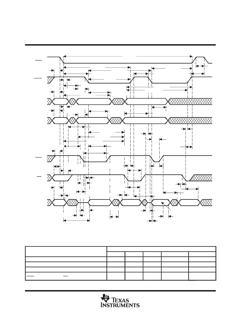
PARAMETER MEASUREMENT INFORMATION
RAS
CASx
A0–A8
WE
TRG
DSF
DQ0–DQ15
tw(RL)P
td(RLCH)
tc(RDWP)
td(RLCL)
tw(CL)
tw(CH)
td(CLRH)
tw(RH
td(CHRL)
tsu(RA)
tsu(CA)
th(RA)
th(RLCA)
1
2
2
3
4
tsu(SFR)
th(SFR)
tsu(SFC)
th(SFC)
tsu(rd)
tsu(WMR)
td(CLWL)
td(CAWL)
td(RLWL)
tsu(WCH)
td(GHD)
ta(R) (see Note A)
tdis(G)
Row
Column
Column
Valid Out
5
Valid Out
ta(C) (see Note A)
td(DCL)
td(DGL)
td(RLCA)
td(CHRL)
th(RDQ)
tsu(DQR)
tsu(TRG)
th(TRG)
td(DCL)
ta(CA) (see Note A)
th(WLD)
tw(TRG)
tsu(WRH)
th(SFC)
tw(WL)
td(CLGH)
tsu(DWL)
td(DGL)
th(RWM)
td(CLGH)
tw(TRG)
5
tsu(DWL)
th(WLD)
td(GHD)
th(CLCA)
tsu(SFC)
tsu(WCH)
ta(CP) (see Note A)
ta(C) (see Note A)
ta(G) (see Note A)
td(CACH)
td(CARH)
NOTES: A. Output can go from the high-impedance state to an invalid-data state prior to the specified access time.
B. A read or a write cycle can be intermixed with read-modify-write cycles as long as the read and write timing specifications are
not violated.
Figure 36. Enhanced-Page-Mode Read-Modify-Write-Cycle Timing
Table 11. Enhanced-Page-Mode Read-Modify-Write-Cycle State Table
CYCLE
STATE
1
2
3
4
5
Write operation (nonmasked)
L
L
H
Don’t care
Valid data
Write operation with nonpersistent write-per-bit
L
L
L
Write mask
Valid data
Write operation with persistent write-per-bit
L
L
L
Don’t care
Valid data
Load write-mask register on either the first falling edge of
CASx or the falling edge of WE, whichever occurs later.
Load-write-mask-register cycle puts the device in the persistent write-per-bit mode. Column address at the falling edge of CASx is a don’t care
during this cycle.
H
L
H
Don’t care
Write mask
相關(guān)PDF資料 |
PDF描述 |
|---|---|
| SMJ55166 | 262144 BY 16-BIT MULTIPORT VIDEO RAM |
| SMJ626162 | 524288 BY 16-BIT BY 2-BANK SYNCHRONOUS DYNAMIC RANDOM-ACCESS MEMORY |
| SML-010DT | Chip LEDs with reflectors |
| SML-010FT | Chip LEDs with reflectors |
| SML-010JT | Chip LEDs with reflectors |
相關(guān)代理商/技術(shù)參數(shù) |
參數(shù)描述 |
|---|---|
| SMJ55166 | 制造商:TI 制造商全稱:Texas Instruments 功能描述:262144 BY 16-BIT MULTIPORT VIDEO RAM |
| SMJ55166-75HKCM | 制造商:Micross Components 功能描述:DRAM 2KX16 "VIDEO RAM" - Bulk |
| SMJ5821TS50 | 制造商:MICRO SEMI 功能描述:New |
| SMJ5C1008-25JDCM | 制造商:Rochester Electronics LLC 功能描述:- Bulk |
| SMJ5C1008L-25JDCM | 制造商:Texas Instruments 功能描述: |
發(fā)布緊急采購,3分鐘左右您將得到回復(fù)。