- 您現(xiàn)在的位置:買賣IC網(wǎng) > PDF目錄374843 > SMJ55161 (Texas Instruments, Inc.) 262144 BY 16-BIT MULTIPORT VIDEO RAM PDF資料下載
參數(shù)資料
| 型號: | SMJ55161 |
| 廠商: | Texas Instruments, Inc. |
| 英文描述: | 262144 BY 16-BIT MULTIPORT VIDEO RAM |
| 中文描述: | 262144由16位多端口視頻內(nèi)存 |
| 文件頁數(shù): | 26/64頁 |
| 文件大小: | 1505K |
| 代理商: | SMJ55161 |
第1頁第2頁第3頁第4頁第5頁第6頁第7頁第8頁第9頁第10頁第11頁第12頁第13頁第14頁第15頁第16頁第17頁第18頁第19頁第20頁第21頁第22頁第23頁第24頁第25頁當(dāng)前第26頁第27頁第28頁第29頁第30頁第31頁第32頁第33頁第34頁第35頁第36頁第37頁第38頁第39頁第40頁第41頁第42頁第43頁第44頁第45頁第46頁第47頁第48頁第49頁第50頁第51頁第52頁第53頁第54頁第55頁第56頁第57頁第58頁第59頁第60頁第61頁第62頁第63頁第64頁
SMJ55161
262144 BY 16-BIT
MULTIPORT VIDEO RAM
SGMS056D – MAY 1995 – REVISED OCTOBER 1997
26
POST OFFICE BOX 1443
HOUSTON, TEXAS 77251–1443
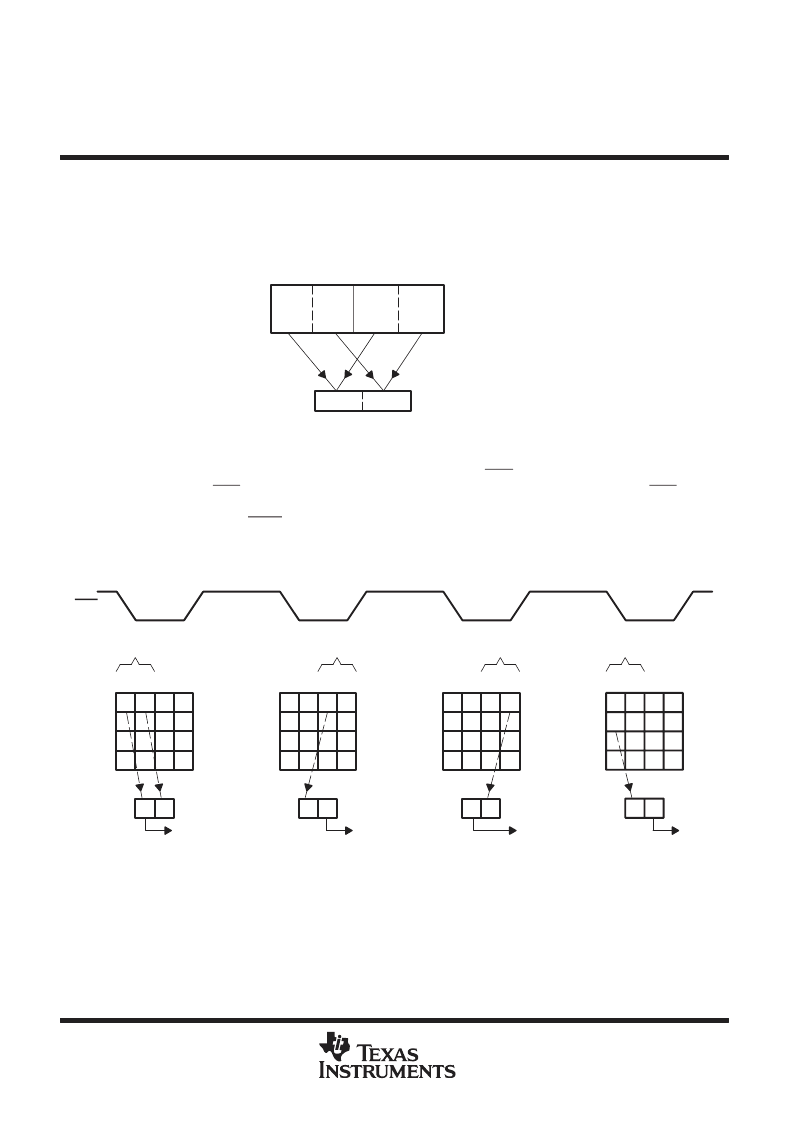
split-register-transfer read
In the split-register-transfer-read operation, the serial-data register is split into halves. The low half contains bits
0–127, and the high half contains bits 128– 255. While one half is being read out of the SAM port, the other
half can be loaded from the memory array.
512
×
512
Memory Array
256-Bit
Data Register
0
255 256
511
0
255
A8 = 0
A8 = 1
Figure 17. Split-Register-Transfer Read
To invoke a split-register-transfer-read cycle, DSF is brought high, TRG is brought low, and both are latched
at the falling edge of RAS. Nine row-address bits (A0–A8) are also latched at the falling edge of RAS to select
one of the 512 rows available for the transfer. Eight of the nine column-address bits (A0–A6 and A8) are latched
at the first falling edge of CASx. Column-address bit A8 selects which half of the row is to be transferred.
Column-address bits A0–A6 selects one of the 127 tap points in the specified half of the SAM. Column-address
bit A7 is ignored, and the split-register transfer is controlled internally to select the inactive register half.
Full XFER
RAS
Split XFER
Split XFER
Split XFER
A
B
0
511
A8 = 0
A
B
0
255
SQ
A
B
C
0
A7 = 0511
A8 = 1
C
B
0
255
A
B
C
D
0
A7 = 1511
A8 = 1
C
D
0
255
SQ
A
B
C
D
E
0 A7 = 0
511
A8 = 0
E
D
0
255
SQ
SQ
DRAM
SAM
A7 shown as internally controlled.
Figure 18. Example of a Split-Register-Transfer Read Operation
A full-register-transfer-read cycle must precede the first split-register-transfer-read cycle to ensure proper
operation. After the full-register-transfer-read cycle, the first split-register-transfer-read cycle can follow
immediately without any minimum SC-clock requirement.
相關(guān)PDF資料 |
PDF描述 |
|---|---|
| SMJ55166 | 262144 BY 16-BIT MULTIPORT VIDEO RAM |
| SMJ626162 | 524288 BY 16-BIT BY 2-BANK SYNCHRONOUS DYNAMIC RANDOM-ACCESS MEMORY |
| SML-010DT | Chip LEDs with reflectors |
| SML-010FT | Chip LEDs with reflectors |
| SML-010JT | Chip LEDs with reflectors |
相關(guān)代理商/技術(shù)參數(shù) |
參數(shù)描述 |
|---|---|
| SMJ55166 | 制造商:TI 制造商全稱:Texas Instruments 功能描述:262144 BY 16-BIT MULTIPORT VIDEO RAM |
| SMJ55166-75HKCM | 制造商:Micross Components 功能描述:DRAM 2KX16 "VIDEO RAM" - Bulk |
| SMJ5821TS50 | 制造商:MICRO SEMI 功能描述:New |
| SMJ5C1008-25JDCM | 制造商:Rochester Electronics LLC 功能描述:- Bulk |
| SMJ5C1008L-25JDCM | 制造商:Texas Instruments 功能描述: |
發(fā)布緊急采購,3分鐘左右您將得到回復(fù)。