- 您現(xiàn)在的位置:買賣IC網(wǎng) > PDF目錄374843 > SMJ55161 (Texas Instruments, Inc.) 262144 BY 16-BIT MULTIPORT VIDEO RAM PDF資料下載
參數(shù)資料
| 型號: | SMJ55161 |
| 廠商: | Texas Instruments, Inc. |
| 英文描述: | 262144 BY 16-BIT MULTIPORT VIDEO RAM |
| 中文描述: | 262144由16位多端口視頻內(nèi)存 |
| 文件頁數(shù): | 34/64頁 |
| 文件大小: | 1505K |
| 代理商: | SMJ55161 |
第1頁第2頁第3頁第4頁第5頁第6頁第7頁第8頁第9頁第10頁第11頁第12頁第13頁第14頁第15頁第16頁第17頁第18頁第19頁第20頁第21頁第22頁第23頁第24頁第25頁第26頁第27頁第28頁第29頁第30頁第31頁第32頁第33頁當前第34頁第35頁第36頁第37頁第38頁第39頁第40頁第41頁第42頁第43頁第44頁第45頁第46頁第47頁第48頁第49頁第50頁第51頁第52頁第53頁第54頁第55頁第56頁第57頁第58頁第59頁第60頁第61頁第62頁第63頁第64頁
SMJ55161
262144 BY 16-BIT
MULTIPORT VIDEO RAM
SGMS056D – MAY 1995 – REVISED OCTOBER 1997
34
POST OFFICE BOX 1443
HOUSTON, TEXAS 77251–1443
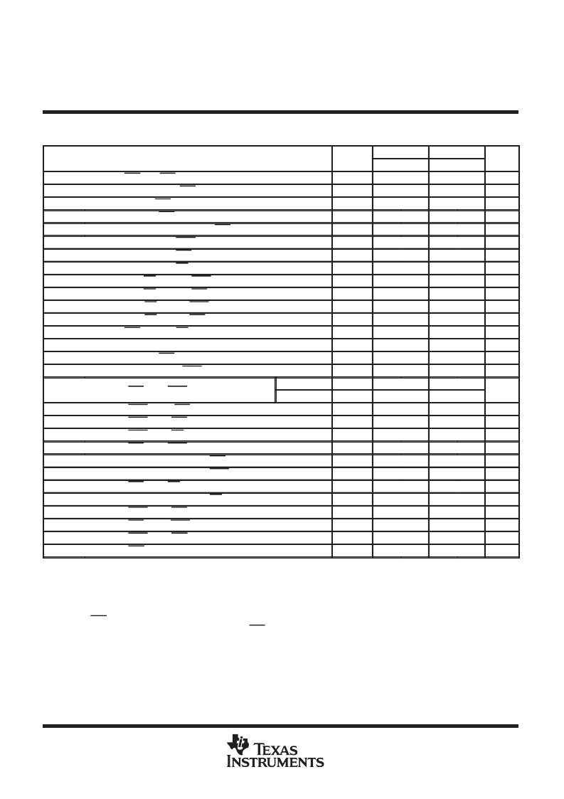
timing requirements over recommended ranges of supply voltage and operating free-air
temperature (continued)
ALT.
’55161-75
MIN
’55161-80
MIN
UNIT
SYMBOL
MAX
MAX
th(TRG)
th(RWM)
th(RDQ)
th(SFR)
th(RLCA)
th(CLD)
th(RLD)
th(WLD)
th(CHrd)
th(RHrd)
th(CLW)
th(RLW)
th(WLG)
th(SHSQ)
th(RSF)
th(CLQ)
Hold time, TRG after RAS low
tTHH
tRWH
tMH
tRFH
tAR
tDH
tDHR
tDH
tRCH
tRRH
tWCH
tWCR
tOEH
tSOH
tFHR
tDHC
tCSH
tCHR
tCRP
tRSH
tCWD
tRCD
tRAL
tCAL
tRWD
tAWD
tCSR
tRPC
15
15
ns
Hold time, write mask after RAS low
15
15
ns
Hold time, DQ after RAS low (write-mask operation)
15
15
ns
Hold time, DSF after RAS low
10
10
ns
Hold time, column address valid after RAS low (see Note 12)
33
35
ns
Hold time, data valid after CASx low
15
15
ns
Hold time, data valid after RAS low (see Note 12)
35
35
ns
Hold time, data valid after WE low
15
15
ns
Hold time, read, WE high after CASx high (see Note 13)
0
0
ns
Hold time, read, WE high after RAS high (see Note 13)
0
0
ns
Hold time, write, WE low after CASx low
15
15
ns
Hold time, write, WE low after RAS low (see Note 12)
35
35
ns
Hold time, TRG high after WE low (see Note 14)
10
10
ns
Hold time, SQ valid after SC high
2
2
ns
Hold time, DSF after RAS low
35
35
ns
Hold time, output valid after CASx low
0
0
ns
td(RLCH)
Dela time RAS lo
Delay time, RAS low to CASx high
to CAS high
75
80
ns
(See Note 15)
13
15
td(CHRL)
td(CLRH)
td(CLWL)
td(RLCL)
td(CARH)
td(CACH)
td(RLWL)
td(CAWL)
td(CLRL)
td(RHCL)
td(CLGH)
td(GHD)
Timing measurements are referenced to VIL MAX and VIH MIN.
NOTES: 12. The minimum value is measured when td(RLCL) is set to td(RLCL) MIN as a reference.
13. Either th(RHrd) or td(CHrd) must be satisfied for a read cycle.
14. Output-enable-controlled write. Output remains in the high-impedance state for the entire cycle.
15. CBR refresh operation only
16. Read-modify-write operation only
17. TRG must disable the output buffers prior to applying data to the DQ pins.
18. The maximum value is specified only to assure RAS access time.
Delay time, CASx high to RAS low
0
0
ns
Delay time, CASx low to RAS high
20
20
ns
Delay time, CASx low to WE low (see Notes 16 and 17)
48
50
ns
Delay time, RAS low to CASx low (see Note 18)
20
50
20
60
ns
Delay time, column address valid to RAS high
38
40
ns
Delay time, column address valid to CASx high
38
40
ns
Delay time, RAS low to WE low (see Note 16)
100
105
ns
Delay time, column address valid to WE low (see Note 16)
63
65
ns
Delay time, CASx low to RAS low (see Note 15)
0
0
ns
Delay time, RAS high to CASx low (see Note 15)
0
0
ns
Delay time, CASx low to TRG high for DRAM read cycles
20
20
ns
Delay time, TRG high before data applied at DQ
tOED
15
15
ns
相關(guān)PDF資料 |
PDF描述 |
|---|---|
| SMJ55166 | 262144 BY 16-BIT MULTIPORT VIDEO RAM |
| SMJ626162 | 524288 BY 16-BIT BY 2-BANK SYNCHRONOUS DYNAMIC RANDOM-ACCESS MEMORY |
| SML-010DT | Chip LEDs with reflectors |
| SML-010FT | Chip LEDs with reflectors |
| SML-010JT | Chip LEDs with reflectors |
相關(guān)代理商/技術(shù)參數(shù) |
參數(shù)描述 |
|---|---|
| SMJ55166 | 制造商:TI 制造商全稱:Texas Instruments 功能描述:262144 BY 16-BIT MULTIPORT VIDEO RAM |
| SMJ55166-75HKCM | 制造商:Micross Components 功能描述:DRAM 2KX16 "VIDEO RAM" - Bulk |
| SMJ5821TS50 | 制造商:MICRO SEMI 功能描述:New |
| SMJ5C1008-25JDCM | 制造商:Rochester Electronics LLC 功能描述:- Bulk |
| SMJ5C1008L-25JDCM | 制造商:Texas Instruments 功能描述: |
發(fā)布緊急采購,3分鐘左右您將得到回復。