- 您現(xiàn)在的位置:買賣IC網(wǎng) > PDF目錄384756 > MT49H16M18C (Micron Technology, Inc.) 288Mb SIO REDUCED LATENCY(RLDRAM II) PDF資料下載
參數(shù)資料
| 型號(hào): | MT49H16M18C |
| 廠商: | Micron Technology, Inc. |
| 英文描述: | 288Mb SIO REDUCED LATENCY(RLDRAM II) |
| 中文描述: | 288Mb二氧化硅約化延遲(延遲DRAM二) |
| 文件頁數(shù): | 38/44頁 |
| 文件大小: | 1117K |
| 代理商: | MT49H16M18C |
第1頁第2頁第3頁第4頁第5頁第6頁第7頁第8頁第9頁第10頁第11頁第12頁第13頁第14頁第15頁第16頁第17頁第18頁第19頁第20頁第21頁第22頁第23頁第24頁第25頁第26頁第27頁第28頁第29頁第30頁第31頁第32頁第33頁第34頁第35頁第36頁第37頁當(dāng)前第38頁第39頁第40頁第41頁第42頁第43頁第44頁
16 MEG x 18, 32 MEG x 9
2.5V V
EXT
, 1.8V V
DD
, HSTL, SIO, RLDRAM II
pdf: 09005aef80a41b59/zip: 09005aef811ba111
MT49H8M18C_2.fm - Rev. F 11/04 EN
Micron Technology, Inc., reserves the right to change products or specifications without notice.
2004 Micron Technology, Inc. All rights reserved.
38
NOTE:
1.
t
CS and
t
CH refer to the setup and hold time requirements of latching data from the boundary scan register.
NOTE:
1. All voltages referenced to V
SS
(GND).
2. Overshoot:
V
IH
(
AC
)
≤
V
DD
+ 0.7V for t
≤
t
CK/2.
Undershoot: V
IL
(
AC
)
≥
-0.5V for t
≤
t
CK/2.
During normal operation, V
DD
Q must not exceed V
DD
.
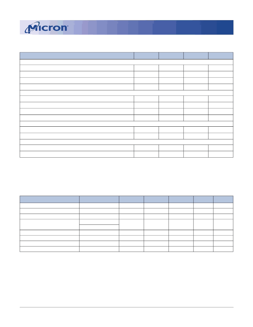
Table 13:
Note 1; +0°C
≤
T
C
≤
+95°C; +1.7V
≤
V
DD
≤
+1.9V
TAP AC Electrical Characteristics
DESCRIPTION
Clock
Clock cycle time
SYMBOL
MIN
MAX
UNITS
t
THTH
f
TF
t
THTL
t
TLTH
20
ns
Clock frequency
50
MHz
Clock HIGH time
10
ns
Clock LOW time
10
ns
Output Times
TCK LOW to TDO unknown
t
TLOX
t
TLOV
t
DVTH
t
THDX
0
ns
TCK LOW to TDO valid
10
ns
TDI valid to TCK HIGH
5
ns
TCK HIGH to TDI invalid
5
ns
Setup Times
TMS setup
t
MVTH
t
CS
5
ns
Capture setup
5
ns
Hold Times
TMS hold
t
THMX
t
CH
5
ns
Capture hold
5
ns
Table 14:
+0°C
≤
T
C
≤
+95°C; +1.7V
≤
V
DD
≤
+1.9V, unless otherwise noted
TAP DC Electrical Characteristics and Operating Conditions
DESCRIPTION
CONDITIONS
SYMBOL
V
IH
V
IL
IL
I
IL
O
MIN
MAX
V
DD
+ 0.3
V
REF
- 0.15
5.0
5.0
UNITS
V
V
μA
μA
NOTES
1, 2
1, 2
Input High (Logic 1) Voltage
Input Low (Logic 0) Voltage
Input Leakage Current
Output Leakage Current
V
REF
+ 0.15
V
SS
Q - 0.3
-5.0
-5.0
0V
≤
V
IN
≤
V
DD
Output disabled,
0V
≤
V
IN
≤
V
DD
Q
I
OLC
= 100μA
I
OLT
= 2mA
|I
OHC
| = 100μA
|I
OHT
| = 2mA
Output Low Voltage
Output Low Voltage
Output High Voltage
Output High Voltage
V
OL
1
V
OL
2
V
OH
1
V
OH
2
0.2
0.4
V
V
V
V
1
1
1
1
V
DD
Q - 0.2
V
DD
Q - 0.4
相關(guān)PDF資料 |
PDF描述 |
|---|---|
| MT49H16M18CFM-xx | 288Mb SIO REDUCED LATENCY(RLDRAM II) |
| MT49H32M9C | 288Mb SIO REDUCED LATENCY(RLDRAM II) |
| MT49H32M9CFM-xx | 288Mb SIO REDUCED LATENCY(RLDRAM II) |
| MT4C1004J | 4 Meg x 1 FPM DRAM(4 M x 1快速頁面模式動(dòng)態(tài)RAM) |
| MT4C4001STG-6 | standard or self refresh |
相關(guān)代理商/技術(shù)參數(shù) |
參數(shù)描述 |
|---|---|
| MT49H16M18CBM-25 | 制造商:Micron Technology Inc 功能描述: |
| MT49H16M18CBM-25 TR | 制造商:Micron Technology Inc 功能描述:16MX18 RLDRAM PLASTIC PBF FBGA 1.8V SEPARATE I/O 8 BANKS - Tape and Reel |
| MT49H16M18CBM-33 IT | 制造商:Micron Technology Inc 功能描述: |
發(fā)布緊急采購,3分鐘左右您將得到回復(fù)。