- 您現(xiàn)在的位置:買賣IC網(wǎng) > PDF目錄384756 > MT49H16M18C (Micron Technology, Inc.) 288Mb SIO REDUCED LATENCY(RLDRAM II) PDF資料下載
參數(shù)資料
| 型號: | MT49H16M18C |
| 廠商: | Micron Technology, Inc. |
| 英文描述: | 288Mb SIO REDUCED LATENCY(RLDRAM II) |
| 中文描述: | 288Mb二氧化硅約化延遲(延遲DRAM二) |
| 文件頁數(shù): | 15/44頁 |
| 文件大小: | 1117K |
| 代理商: | MT49H16M18C |
第1頁第2頁第3頁第4頁第5頁第6頁第7頁第8頁第9頁第10頁第11頁第12頁第13頁第14頁當前第15頁第16頁第17頁第18頁第19頁第20頁第21頁第22頁第23頁第24頁第25頁第26頁第27頁第28頁第29頁第30頁第31頁第32頁第33頁第34頁第35頁第36頁第37頁第38頁第39頁第40頁第41頁第42頁第43頁第44頁
16 MEG x 18, 32 MEG x 9
2.5V V
EXT
, 1.8V V
DD
, HSTL, SIO, RLDRAM II
pdf: 09005aef80a41b59/zip: 09005aef811ba111
MT49H8M18C_2.fm - Rev. F 11/04 EN
Micron Technology, Inc., reserves the right to change products or specifications without notice.
2004 Micron Technology, Inc. All rights reserved.
15
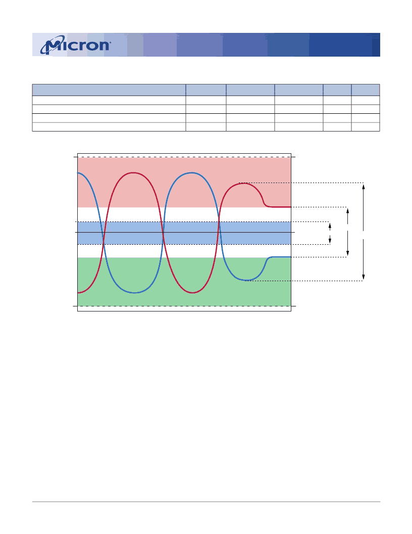
Figure 7: Clock Input
NOTE:
1. DKx and DKx# have the same requirements as CK and CK#.
2. All voltages referenced to V
SS
.
3. Tests for AC timing, I
DD
, and electrical AC and DC characteristics may be conducted at nominal reference/supply voltage
levels, but the related specifications and device operations are tested for the full voltage range specified.
4. Outputs (except for I
DD
measurements) measured with equivalent load.
5. AC timing and I
DD
tests may use a V
IL
-to-V
IH
swing of up to 1.5V in the test environment, but input timing is still refer-
enced to V
REF
(or to the crossing point for CK/CK#), and parameter specifications are tested for the specified AC input
levels under normal use conditions. The minimum slew rate for the input signals used to test the device is 2 V/ns in the
range between V
IL
(
AC
) and V
IH
(
AC
).
6. The AC and DC input level specifications are as defined in the HSTL Standard (i.e., the receiver will effectively switch as a
result of the signal crossing the AC input level, and will remain in that state as long as the signal does not ring back
above [below] the DC input LOW [HIGH] level).
7. The CK/CK# input reference level (for timing referenced to CK/CK#) is the point at which CK and CK# cross. The input
reference level for signals other than CK/CK# is V
REF
.
8. CK and CK# input slew rate must be
≥
2 V/ns (
≥
4 V/ns if measured differentially).
9. V
ID
is the magnitude of the difference between the input level on CK and the input level on CK#.
10. The value of V
IX
is expected to equal V
DD
Q/2 of the transmitting device and must track variations in the DC level of the
same.
11. CK and CK# must cross within this region.
12. CK and CK# must meet at least V
ID
(
DC
) MIN when static and centered around V
DD
Q/2.
13. Minimum peak-to-peak swing.
Table 7:
Notes 1–8
Clock Input Operating Conditions
PARAMETER/CONDITION
SYMBOL
V
IN
(
DC
)
V
ID
(
DC
)
V
ID
(
AC
)
V
IX
(
AC
)
MIN
-0.3
0.2
0.4
MAX
UNITS
V
V
V
V
NOTES
Clock Input Voltage Level; CK and CK#
Clock Input Differential Voltage; CK and CK#
Clock Input Differential Voltage; CK and CK#
Clock Input Crossing Point Voltage; CK and CK#
V
DD
Q + 0.3
V
DD
Q + 0.6
V
DD
Q + 0.6
V
DD
Q/2 + 0.15
9
9
V
DD
Q/2 - 0.15
10
CK
CK#
V
IN(DC)
MAX
11
12
Maximum Clock Level
Minimum Clock Level
13
V
IN(DC)
MIN
V
DD
Q/2
V
DD
Q/2 + 0.15
V
DD
Q/2 - 0.15
X
X
V
IX(AC)
MIN
X
X
V
ID(AC)
V
ID(DC)
V
IX(AC)
MAX
相關PDF資料 |
PDF描述 |
|---|---|
| MT49H16M18CFM-xx | 288Mb SIO REDUCED LATENCY(RLDRAM II) |
| MT49H32M9C | 288Mb SIO REDUCED LATENCY(RLDRAM II) |
| MT49H32M9CFM-xx | 288Mb SIO REDUCED LATENCY(RLDRAM II) |
| MT4C1004J | 4 Meg x 1 FPM DRAM(4 M x 1快速頁面模式動態(tài)RAM) |
| MT4C4001STG-6 | standard or self refresh |
相關代理商/技術參數(shù) |
參數(shù)描述 |
|---|---|
| MT49H16M18CBM-25 | 制造商:Micron Technology Inc 功能描述: |
| MT49H16M18CBM-25 TR | 制造商:Micron Technology Inc 功能描述:16MX18 RLDRAM PLASTIC PBF FBGA 1.8V SEPARATE I/O 8 BANKS - Tape and Reel |
| MT49H16M18CBM-33 IT | 制造商:Micron Technology Inc 功能描述: |
發(fā)布緊急采購,3分鐘左右您將得到回復。