- 您現(xiàn)在的位置:買賣IC網(wǎng) > PDF目錄384756 > MT49H16M18C (Micron Technology, Inc.) 288Mb SIO REDUCED LATENCY(RLDRAM II) PDF資料下載
參數(shù)資料
| 型號: | MT49H16M18C |
| 廠商: | Micron Technology, Inc. |
| 英文描述: | 288Mb SIO REDUCED LATENCY(RLDRAM II) |
| 中文描述: | 288Mb二氧化硅約化延遲(延遲DRAM二) |
| 文件頁數(shù): | 35/44頁 |
| 文件大?。?/td> | 1117K |
| 代理商: | MT49H16M18C |
第1頁第2頁第3頁第4頁第5頁第6頁第7頁第8頁第9頁第10頁第11頁第12頁第13頁第14頁第15頁第16頁第17頁第18頁第19頁第20頁第21頁第22頁第23頁第24頁第25頁第26頁第27頁第28頁第29頁第30頁第31頁第32頁第33頁第34頁當前第35頁第36頁第37頁第38頁第39頁第40頁第41頁第42頁第43頁第44頁
16 MEG x 18, 32 MEG x 9
2.5V V
EXT
, 1.8V V
DD
, HSTL, SIO, RLDRAM II
pdf: 09005aef80a41b59/zip: 09005aef811ba111
MT49H8M18C_2.fm - Rev. F 11/04 EN
Micron Technology, Inc., reserves the right to change products or specifications without notice.
2004 Micron Technology, Inc. All rights reserved.
35
IEEE 1149.1 Serial Boundary Scan (JTAG)
RLDRAM incorporates a serial boundary scan test
access port (TAP). This port operates in accordance
with IEEE Standard 1149.1-2001. The TAP operates
using logic levels associated with the V
DD
Q supply.
RLDRAM contains a TAP controller, instruction reg-
ister, boundary scan register, bypass register, and ID
register.
Disabling the JTAG Feature
It is possible to operate RLDRAM without using the
JTAG feature. To disable the TAP controller, TCK must
be tied LOW (V
SS
) to prevent clocking of the device.
TDI and TMS are internally pulled up and may be
unconnected. They may alternately be connected to
V
DD
through a pull-up resistor. TDO should be left
unconnected. Upon power-up, the device will come up
in a reset state, which will not interfere with the opera-
tion of the device.
Test Access Port (TAP)
Test Clock (TCK)
The test clock is used only with the TAP controller.
All inputs are captured on the rising edge of TCK. All
outputs are driven from the falling edge of TCK.
Test Mode Select (TMS)
The TMS input is used to give commands to the TAP
controller and is sampled on the rising edge of TCK. It
is allowable to leave this ball unconnected if the TAP is
not used. The ball is pulled up internally, resulting in a
logic HIGH level.
Test Data-In (TDI)
The TDI ball is used to serially input information
into the registers and can be connected to the input of
any of the registers. The register between TDI and TDO
is chosen by the instruction that is loaded into the TAP
instruction register. For information on loading the
instruction register, see Figure 38. TDI is internally
pulled up and can be unconnected if the TAP is unused
in an application. TDI is connected to the most signifi-
cant bit (MSB) of any register (see Figure 39).
Test Data-Out (TDO)
The TDO output ball is used to serially clock data-
out from the registers. The output is active depending
upon the current state of the TAP state machine (see
Figure 38). The output changes on the falling edge of
TCK. TDO is connected to the least significant bit
(LSB) of any register (see Figure 39).
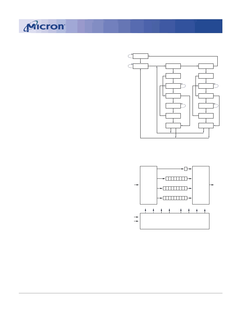
Figure 38: TAP Controller State
Diagram
Figure 39: TAP Controller Block
Diagram
NOTE:
x = 112 for all configurations.
Performing a TAP RESET
A reset is performed by forcing TMS HIGH (V
DD
) for
five rising edges of TCK. This RESET does not affect the
operation of the RLDRAM and may be performed
while the RLDRAM is operating.
At power-up, the TAP is reset internally to ensure
that TDO comes up in a High-Z state.
TEST-LOGIC
RESET
RUN-TEST/
IDLE
SELECT
DR-SCAN
SELECT
IR-SCAN
CAPTURE-DR
SHIFT-DR
CAPTURE-IR
SHIFT-IR
EXIT1-DR
PAUSE-DR
EXIT1-IR
PAUSE-IR
EXIT2-DR
UPDATE-DR
EXIT2-IR
UPDATE-IR
1
1
1
0
1
1
0
0
1
1
1
0
0
0
0
0
0
0
0
0
1
0
1
1
0
1
0
1
1
1
1
0
Bypass Register
0
Instruction Register
0
1
2
3
4
5
6
7
Identification Register
0
1
2
29
30
31
.
.
.
Boundary Scan Register
0
1
2
.
.
x
.
.
.
Selection
Circuitry
Selection
Circuitry
TCK
TMS
TAP Controller
TDI
TDO
相關PDF資料 |
PDF描述 |
|---|---|
| MT49H16M18CFM-xx | 288Mb SIO REDUCED LATENCY(RLDRAM II) |
| MT49H32M9C | 288Mb SIO REDUCED LATENCY(RLDRAM II) |
| MT49H32M9CFM-xx | 288Mb SIO REDUCED LATENCY(RLDRAM II) |
| MT4C1004J | 4 Meg x 1 FPM DRAM(4 M x 1快速頁面模式動態(tài)RAM) |
| MT4C4001STG-6 | standard or self refresh |
相關代理商/技術參數(shù) |
參數(shù)描述 |
|---|---|
| MT49H16M18CBM-25 | 制造商:Micron Technology Inc 功能描述: |
| MT49H16M18CBM-25 TR | 制造商:Micron Technology Inc 功能描述:16MX18 RLDRAM PLASTIC PBF FBGA 1.8V SEPARATE I/O 8 BANKS - Tape and Reel |
| MT49H16M18CBM-33 IT | 制造商:Micron Technology Inc 功能描述: |
發(fā)布緊急采購,3分鐘左右您將得到回復。