- 您現(xiàn)在的位置:買賣IC網(wǎng) > PDF目錄370849 > M37902FJCHP (Mitsubishi Electric Corporation) SINGLE-CHIP 16-BIT CMOS MICROCOMPUTER PDF資料下載
參數(shù)資料
| 型號: | M37902FJCHP |
| 廠商: | Mitsubishi Electric Corporation |
| 英文描述: | SINGLE-CHIP 16-BIT CMOS MICROCOMPUTER |
| 中文描述: | 單片16位CMOS微機(jī) |
| 文件頁數(shù): | 92/143頁 |
| 文件大小: | 1463K |
| 代理商: | M37902FJCHP |
第1頁第2頁第3頁第4頁第5頁第6頁第7頁第8頁第9頁第10頁第11頁第12頁第13頁第14頁第15頁第16頁第17頁第18頁第19頁第20頁第21頁第22頁第23頁第24頁第25頁第26頁第27頁第28頁第29頁第30頁第31頁第32頁第33頁第34頁第35頁第36頁第37頁第38頁第39頁第40頁第41頁第42頁第43頁第44頁第45頁第46頁第47頁第48頁第49頁第50頁第51頁第52頁第53頁第54頁第55頁第56頁第57頁第58頁第59頁第60頁第61頁第62頁第63頁第64頁第65頁第66頁第67頁第68頁第69頁第70頁第71頁第72頁第73頁第74頁第75頁第76頁第77頁第78頁第79頁第80頁第81頁第82頁第83頁第84頁第85頁第86頁第87頁第88頁第89頁第90頁第91頁當(dāng)前第92頁第93頁第94頁第95頁第96頁第97頁第98頁第99頁第100頁第101頁第102頁第103頁第104頁第105頁第106頁第107頁第108頁第109頁第110頁第111頁第112頁第113頁第114頁第115頁第116頁第117頁第118頁第119頁第120頁第121頁第122頁第123頁第124頁第125頁第126頁第127頁第128頁第129頁第130頁第131頁第132頁第133頁第134頁第135頁第136頁第137頁第138頁第139頁第140頁第141頁第142頁第143頁
M37902FCCHP, M37902FGCHP, M37902FJCHP
SINGLE-CHIP 16-BIT CMOS MICROCOMPUTER
MITSUBISHI MICROCOMPUTERS
92
CLOCK GENERATING CIRCUIT
Figure 98 shows the block diagram of the clock generating circuit.
The clock generating circuit consists of the clock oscillation circuit,
PLL frequency multiplier (PLL circuit), system clock switch circuit,
peripheral devices’ clock switch circuit, clock divider, standby control
circuit, etc. As control registers for the clock generating circuit, also,
the clock control register (address BC
16
), particular function select
register 0 (address 62
16
) are provided. (See Figures 99 and 100.)
As shown in Figure 98, clocks used in the CPU, BIU, peripheral de-
vices, watchdog timer (in other words, clocks
φ
CPU
,
φ
BIU
, f
1
to f
4096
,
Wf
32
, Wf
512
) are made from system clock f
sys
. System clock f
sys
can
be selected between fX
IN
(in other words, a clock input from pin X
IN)
and f
PLL
(in other words, an output clock generated by the PLL cir-
cuit). By setting the clock
φ
1
output select bit (bit 7 of the processor
mode register 0) to “1”, also, system clock f
sys
can be output from
port pin P4
1
, as clock
φ
1
.
The PLL circuit’s operation, system clock (f
sys
) selection, and divide
ratio selection for peripheral devices’ clocks (f
1
to f
4096
) are con-
trolled by the clock control register. The following describes about
these control.
Bit 1 of the clock control register (the PLL circuit operation enable bit)
selects the PLL circuit’s operation (stopped/active). When this bit is
set to “1”, pin V
CONT
will becomes valid, and the PLL circuit will oper-
ate. At reset, the PLL circuit operation enable bit becomes “1”. (In this
case, the PLL circuit operates.) When not using the PLL circuit, be
sure to clear the PLL circuit operation enable bit to “0” (stopped). At
the
STP
instruction execution or while the flash memory parallel I/O
mode is set, the PLL circuit stops its operation, and pin V
CONT
is in-
valid, regardless of this bit 1’s status.
Bits 2 and 3 of the clock control register (the PLL multiplication ratio
select bits) select the ratio of f
PLL
/fX
IN
. The PLL multiplication ratio
must be set so that the frequency of the PLL output clock (f
PLL
) must
be in the range from 10 MHz to 26 MHz. At reset, the PLL multiplica-
tion ratio select bits become “0,1” (
2). The change of the multipli-
cation ratio must be performed while input clock fX
IN
is set as system
clock. (In this case, bit 5 of the clock control register = “0”.) After that,
be sure to wait that the operation-stabilizing time of the PLL circuit
has passed, and switch the system clock to the PLL output clock
(f
PLL
). (In other words, set bit 5 to “1”.) Note that, after reset, the PLL
multiplication ratio select bits are allowed to be changed only once.
Bit 5 of the clock control register is the system clock select bit, and
fX
IN
is selected as the system clock when bit 5 = “0”. On the other
hand, when bit 5 = “1”, the PLL output clock (f
PLL
) is selected. At re-
set, the system clock select bit becomes “0”. When selecting f
PLL
, be
sure that the PLL circuit’s operation has been stabilized properly, and
then, set the system clock select bit to “1”. Also, when the PLL circuit
operation enable bit is cleared to “0” (the PLL circuit is stopped.), the
system clock select bit will automatically be cleared to “0”. Note that
a value of “1” cannot be written to the system clock select bit while
the PLL circuit operation enable bit =“0”.
Table 15 lists the f
sys
selection.
Bits 6 and 7 of the clock control register are the peripheral devices’
clock select bits 0, 1, and these bits select the multiplication ratio of
(f
1
to f
4096
)/(f
sys
).
Table 16 lists the internal peripheral devices’ operation clock fre-
quency. At reset, these bits become “0, 0”.
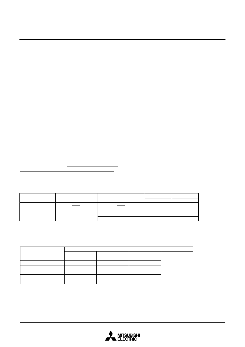
Table 15. f
sys
selection
System clock select bit
(Bit 5)
0
Table 16. Internal peripheral devices’ operation clock frequency
Internal peripheral devices
’
operation clock
f
1
f
2
10 (
3)
11 (
4)
01 (
2)
System clock f
sys
Clock source
fX
IN
f
PLL
f
PLL
f
PLL
Frequency
(Note)
f(X
IN
)
f(X
IN
)
2
f(X
IN
)
3
f(X
IN
)
4
Note:
The PLL multiplication ratio must be set so that the frequency of the PLL output clock (f
PLL
) must be in the range from 10 MHz to 26 MHz.
f(X
IN
) means the frequency of the input clock from pin X
IN
(fX
IN
). After reset, the PLL multiplication ratio select bits are allowed to be
changed only once.
PLL circuit operation enable bit
(Bit 1)
1
1
PLL multiplication ratio select bits
(Bits 3, 2)
(Note)
f
sys
/16
f
sys
/64
f
sys
/512
f
sys
/4096
f
sys
/2
Peripheral devices
’
clock select bits 1, 0 (bits 7, 6)
0 1
(Note)
f
sys
f
sys
f
sys
/8
f
sys
/32
f
sys
/256
f
sys
/2048
1 0
1 1
Note:
When selecting the peripheral devices
’
clock select bits 1, 0 =
“
01
2
”
, be sure that system clock f
sys
does not exceed 13 MHz.
f
16
f
64
f
512
f
4096
f
sys
/2
f
sys
/4
f
sys
/32
f
sys
/128
f
sys
/1024
f
sys
/8192
0 0
f
sys
Do not select.
相關(guān)PDF資料 |
PDF描述 |
|---|---|
| M37905F8CFP | 16-BIT CMOS MICROCOMPUTER |
| M37905F8CSP | 16-BIT CMOS MICROCOMPUTER |
| M37905M4C | DIODE SCHOTTKY DUAL COMMON-ANODE 25V 200mW 0.32V-vf 200mA-IFM 1mA-IF 2uA-IR SOT-323 3K/REEL |
| M37905M4C-XXXFP | 16 BIT CMOS MICROCOMPUTER |
| M37905M4C-XXXSP | 16 BIT CMOS MICROCOMPUTER |
相關(guān)代理商/技術(shù)參數(shù) |
參數(shù)描述 |
|---|---|
| M37903S4CHP | 制造商:RENESAS 制造商全稱:Renesas Technology Corp 功能描述:16-BIT CMOS MICROCOMPUTER |
| M37905F8CFP | 制造商:MITSUBISHI 制造商全稱:Mitsubishi Electric Semiconductor 功能描述:16-BIT CMOS MICROCOMPUTER |
| M37905F8CSP | 制造商:MITSUBISHI 制造商全稱:Mitsubishi Electric Semiconductor 功能描述:16-BIT CMOS MICROCOMPUTER |
| M37905M4C | 制造商:MITSUBISHI 制造商全稱:Mitsubishi Electric Semiconductor 功能描述:16 BIT CMOS MICROCOMPUTER |
| M37905M4C-XXXFP | 制造商:MITSUBISHI 制造商全稱:Mitsubishi Electric Semiconductor 功能描述:16 BIT CMOS MICROCOMPUTER |
發(fā)布緊急采購,3分鐘左右您將得到回復(fù)。