- 您現(xiàn)在的位置:買賣IC網(wǎng) > PDF目錄370849 > M37902FJCHP (Mitsubishi Electric Corporation) SINGLE-CHIP 16-BIT CMOS MICROCOMPUTER PDF資料下載
參數(shù)資料
| 型號: | M37902FJCHP |
| 廠商: | Mitsubishi Electric Corporation |
| 英文描述: | SINGLE-CHIP 16-BIT CMOS MICROCOMPUTER |
| 中文描述: | 單片16位CMOS微機 |
| 文件頁數(shù): | 34/143頁 |
| 文件大小: | 1463K |
| 代理商: | M37902FJCHP |
第1頁第2頁第3頁第4頁第5頁第6頁第7頁第8頁第9頁第10頁第11頁第12頁第13頁第14頁第15頁第16頁第17頁第18頁第19頁第20頁第21頁第22頁第23頁第24頁第25頁第26頁第27頁第28頁第29頁第30頁第31頁第32頁第33頁當前第34頁第35頁第36頁第37頁第38頁第39頁第40頁第41頁第42頁第43頁第44頁第45頁第46頁第47頁第48頁第49頁第50頁第51頁第52頁第53頁第54頁第55頁第56頁第57頁第58頁第59頁第60頁第61頁第62頁第63頁第64頁第65頁第66頁第67頁第68頁第69頁第70頁第71頁第72頁第73頁第74頁第75頁第76頁第77頁第78頁第79頁第80頁第81頁第82頁第83頁第84頁第85頁第86頁第87頁第88頁第89頁第90頁第91頁第92頁第93頁第94頁第95頁第96頁第97頁第98頁第99頁第100頁第101頁第102頁第103頁第104頁第105頁第106頁第107頁第108頁第109頁第110頁第111頁第112頁第113頁第114頁第115頁第116頁第117頁第118頁第119頁第120頁第121頁第122頁第123頁第124頁第125頁第126頁第127頁第128頁第129頁第130頁第131頁第132頁第133頁第134頁第135頁第136頁第137頁第138頁第139頁第140頁第141頁第142頁第143頁
M37902FCCHP, M37902FGCHP, M37902FJCHP
SINGLE-CHIP 16-BIT CMOS MICROCOMPUTER
MITSUBISHI MICROCOMPUTERS
34
Notes 1:
For details of the processor mode setting, see Table 3.
2:
Processor mode bits = bits 0 and 1 of the processor mode register 0 (address 5E
16).
3:
The middle-order/high-order address output pins in the memory expansion or microprocessor mode can be switched to I/O port pins by the address/port
switch select bits of the port function control register (bits 2 to 0 at address 92
16
).
4:
When the external data bus width for the chip select area, CS
2
, has been set to 8 bits, only in the access to area CS
2
, by the multiplexed bus select bit
of the CS
2
control register H (bit 5 at address 85
16
), a multiplexed bus which performs the following operations with the time-sharing method is realized:
Output of address LA
0
to LA
7
Input/Output of data D
0
to D
7
5:
When one of areas CS
1
/CS
2
/CS
3
is accessed under the following conditions, pins D
8
to D
15
enter the floating state, and pin BHW outputs
“
H
”
level.
(They do not become I/O port pins.)
Pin BYTE is at Vss level.
One of bit 2s at addresses 82
16
, 84
16
, 86
16
(the external data bus width select bit of the CS
1
/CS
2
/CS
3
control register L) is set to
“
1
”
(external data bus
width = 8 bits).
6:
In the memory expansion mode, by the corresponding select bits of the processor mode register 0 and 1 (addresses 5E
16
, 5F
16
), port pins P3
0
, P4
0
to
P4
3
can operate as pins for RDY input, ALE output,
φ
1
output, HLDA output, HOLD input, respectively.
In the microprocessor mode, by the above select bits, the above pins (RDY, ALE,
φ
1
, HLDA, HOLD) can operate as port pins P3
0
, P4
0
to P4
3
, respec-
tively.
In the single-chip mode, port pin P4
1
can operate as the
φ
1
output pin by the above select bits.
7:
In the memory expansion mode, port pin P4
4
can operate as the CS
0
output pin by the CS
0
output select bit of the CS
0
control register L (bit 7 at address
80
16
).
8:
In the memory expansion and microprocessor modes, port pins P4
5
to P4
7
can operate as the CS
1
/CS
2
/CS
3
output pins by the CS
i
output select bits (i =
1 to 3) (bit 7s at addresses 82
16
, 84
16
, 86
16
).
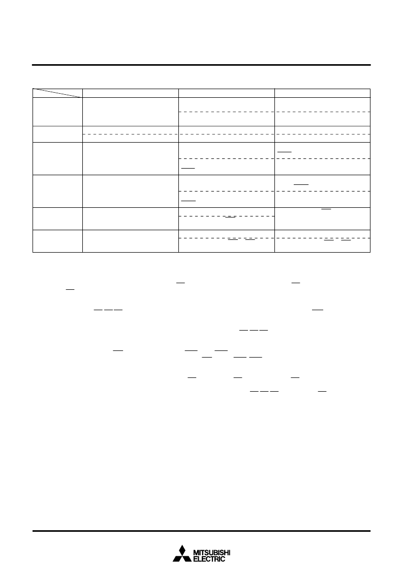
Table 6. Relationship between processor modes, memory area, and port function (2)
Single-chip mode
I/O port pin P4
0
I/O port pin P4
1
Clock
φ
1
is output
(Note 6).
I/O port pin P4
2
I/O port pin P4
3
I/O port pin P4
4
I/O port pins P4
5
to P4
7
Port pin P4
0
Port pin P4
1
Port pin P4
2
Port pin P4
3
Port pin P4
4
Port pins P4
5
to P4
7
Memory expansion mode
I/O port pin P4
0
Address latch enable signal
ALE is output
(Note 6)
.
I/O port pin P4
1
Clock
φ
1
is output
(Note 6)
.
I/O port pin P4
2
Hold acknowledge signal
HLDA is output
(Note 6)
.
I/O port pin P4
3
Hold request signal
HOLD is input
(Note 6)
.
I/O port pin P4
4
Chip select signal CS
0
is output
(Note 7)
.
I/O port pins P4
5
to P4
7
Chip select signals CS
1
to CS
3
are
output
(Note 8)
.
Microprocessor mode
Address latch enable signal
ALE is output.
I/O port pin P4
0
(Note 6)
Clock
φ
1
is output.
I/O port pin P4
1
(Note 6)
Hold acknowledge signal
HLDA is output.
I/O port pin P4
2
(Note 6)
Hold request signal
Signal HOLD is input.
I/O port pin P4
3
(Note 6)
Chip select signal CS
0
is output.
I/O port pin P4
5
to P4
7
Chip select signals CS
1
to CS
3
are
output
(Note 8)
.
相關PDF資料 |
PDF描述 |
|---|---|
| M37905F8CFP | 16-BIT CMOS MICROCOMPUTER |
| M37905F8CSP | 16-BIT CMOS MICROCOMPUTER |
| M37905M4C | DIODE SCHOTTKY DUAL COMMON-ANODE 25V 200mW 0.32V-vf 200mA-IFM 1mA-IF 2uA-IR SOT-323 3K/REEL |
| M37905M4C-XXXFP | 16 BIT CMOS MICROCOMPUTER |
| M37905M4C-XXXSP | 16 BIT CMOS MICROCOMPUTER |
相關代理商/技術參數(shù) |
參數(shù)描述 |
|---|---|
| M37903S4CHP | 制造商:RENESAS 制造商全稱:Renesas Technology Corp 功能描述:16-BIT CMOS MICROCOMPUTER |
| M37905F8CFP | 制造商:MITSUBISHI 制造商全稱:Mitsubishi Electric Semiconductor 功能描述:16-BIT CMOS MICROCOMPUTER |
| M37905F8CSP | 制造商:MITSUBISHI 制造商全稱:Mitsubishi Electric Semiconductor 功能描述:16-BIT CMOS MICROCOMPUTER |
| M37905M4C | 制造商:MITSUBISHI 制造商全稱:Mitsubishi Electric Semiconductor 功能描述:16 BIT CMOS MICROCOMPUTER |
| M37905M4C-XXXFP | 制造商:MITSUBISHI 制造商全稱:Mitsubishi Electric Semiconductor 功能描述:16 BIT CMOS MICROCOMPUTER |
發(fā)布緊急采購,3分鐘左右您將得到回復。