- 您現(xiàn)在的位置:買賣IC網 > PDF目錄370849 > M37902FJCHP (Mitsubishi Electric Corporation) SINGLE-CHIP 16-BIT CMOS MICROCOMPUTER PDF資料下載
參數(shù)資料
| 型號: | M37902FJCHP |
| 廠商: | Mitsubishi Electric Corporation |
| 英文描述: | SINGLE-CHIP 16-BIT CMOS MICROCOMPUTER |
| 中文描述: | 單片16位CMOS微機 |
| 文件頁數(shù): | 38/143頁 |
| 文件大?。?/td> | 1463K |
| 代理商: | M37902FJCHP |
第1頁第2頁第3頁第4頁第5頁第6頁第7頁第8頁第9頁第10頁第11頁第12頁第13頁第14頁第15頁第16頁第17頁第18頁第19頁第20頁第21頁第22頁第23頁第24頁第25頁第26頁第27頁第28頁第29頁第30頁第31頁第32頁第33頁第34頁第35頁第36頁第37頁當前第38頁第39頁第40頁第41頁第42頁第43頁第44頁第45頁第46頁第47頁第48頁第49頁第50頁第51頁第52頁第53頁第54頁第55頁第56頁第57頁第58頁第59頁第60頁第61頁第62頁第63頁第64頁第65頁第66頁第67頁第68頁第69頁第70頁第71頁第72頁第73頁第74頁第75頁第76頁第77頁第78頁第79頁第80頁第81頁第82頁第83頁第84頁第85頁第86頁第87頁第88頁第89頁第90頁第91頁第92頁第93頁第94頁第95頁第96頁第97頁第98頁第99頁第100頁第101頁第102頁第103頁第104頁第105頁第106頁第107頁第108頁第109頁第110頁第111頁第112頁第113頁第114頁第115頁第116頁第117頁第118頁第119頁第120頁第121頁第122頁第123頁第124頁第125頁第126頁第127頁第128頁第129頁第130頁第131頁第132頁第133頁第134頁第135頁第136頁第137頁第138頁第139頁第140頁第141頁第142頁第143頁
M37902FCCHP, M37902FGCHP, M37902FJCHP
SINGLE-CHIP 16-BIT CMOS MICROCOMPUTER
MITSUBISHI MICROCOMPUTERS
38
Chip select wait controller
By the control of the chip select wait controller (CSWC), the chip se-
lect function for the maximum of 4 blocks can be set at the bus ac-
cess to the external area.
Also, by the setting of the CSWC, port pins P4
4
to P4
7
can operate
as chip select output pins (CS
0
to CS
3
).
Figure 27 shows a chip select output waveform example.
This chip select function determines the following items of the chip
select area: start address, address
’
s block size, wait number, exter-
nal data bus width, RDY control validity, burst ROM specification,
recovery cycle insertion validity, and area multiplication validity.
For the external area except for areas CS
0
to CS
3
, the processor
mode registers 0, 1 determine the above items. After reset is re-
moved, when the microcomputer starts it
’
s operation in the micropro-
cessor mode, area CS
0
is automatically selected.
Table 7 lists the function of areas CS
0
to CS
3
.
Figure 28 shows the bit configuration of the CS
0
/CS
1
/CS
2
/CS
3
con-
trol register Ls. These registers determine the following items of a
device to be connected: wait number, external data bus width (
Note:
The external data bus width of area CS
0
is determined by pin BYTE
’
s
level.), RDY control validity, burst ROM access specification, recov-
ery cycle insertion validity, and output validity of CS
0
to CS
3
.
Figure 29 shows the bit configuration of the CS
0
/CS
1
/CS
2
/CS
3
con-
trol register Hs. These registers determine block size, etc. of an ex-
ternal area to be connected. For areas CS
0
to CS
2
, by selecting
mode 1 with the area CSk setting mode select bit, an chip select area
can be set to the external area in bank 0.
Figures 30 shows the bit configuration of the area CS
0
/CS
1
/CS
2
/CS
3
start address registers. For details of these addresses
’
setting, see
Figures 31 to 33.
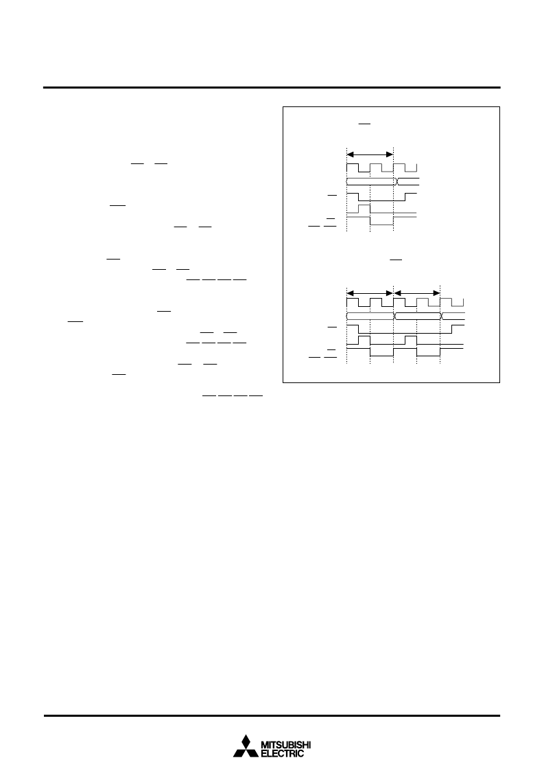
When area CS
i
is accessed
φ
1
A
0
to A
23
ALE
RD,
When the same area CS
i
is accessed sequentially
φ
1
A
0
to A
23
ALE
RD,
Address + 2
One access
cycle
Address
One access
cycle
Address
CS
i
BLW, BHW
BLW, BHW
One access
cycle
CS
i
Fig. 27 Chip select output waveform example
相關PDF資料 |
PDF描述 |
|---|---|
| M37905F8CFP | 16-BIT CMOS MICROCOMPUTER |
| M37905F8CSP | 16-BIT CMOS MICROCOMPUTER |
| M37905M4C | DIODE SCHOTTKY DUAL COMMON-ANODE 25V 200mW 0.32V-vf 200mA-IFM 1mA-IF 2uA-IR SOT-323 3K/REEL |
| M37905M4C-XXXFP | 16 BIT CMOS MICROCOMPUTER |
| M37905M4C-XXXSP | 16 BIT CMOS MICROCOMPUTER |
相關代理商/技術參數(shù) |
參數(shù)描述 |
|---|---|
| M37903S4CHP | 制造商:RENESAS 制造商全稱:Renesas Technology Corp 功能描述:16-BIT CMOS MICROCOMPUTER |
| M37905F8CFP | 制造商:MITSUBISHI 制造商全稱:Mitsubishi Electric Semiconductor 功能描述:16-BIT CMOS MICROCOMPUTER |
| M37905F8CSP | 制造商:MITSUBISHI 制造商全稱:Mitsubishi Electric Semiconductor 功能描述:16-BIT CMOS MICROCOMPUTER |
| M37905M4C | 制造商:MITSUBISHI 制造商全稱:Mitsubishi Electric Semiconductor 功能描述:16 BIT CMOS MICROCOMPUTER |
| M37905M4C-XXXFP | 制造商:MITSUBISHI 制造商全稱:Mitsubishi Electric Semiconductor 功能描述:16 BIT CMOS MICROCOMPUTER |
發(fā)布緊急采購,3分鐘左右您將得到回復。