- 您現(xiàn)在的位置:買賣IC網(wǎng) > PDF目錄370849 > M37902FJCHP (Mitsubishi Electric Corporation) SINGLE-CHIP 16-BIT CMOS MICROCOMPUTER PDF資料下載
參數(shù)資料
| 型號: | M37902FJCHP |
| 廠商: | Mitsubishi Electric Corporation |
| 英文描述: | SINGLE-CHIP 16-BIT CMOS MICROCOMPUTER |
| 中文描述: | 單片16位CMOS微機(jī) |
| 文件頁數(shù): | 32/143頁 |
| 文件大小: | 1463K |
| 代理商: | M37902FJCHP |
第1頁第2頁第3頁第4頁第5頁第6頁第7頁第8頁第9頁第10頁第11頁第12頁第13頁第14頁第15頁第16頁第17頁第18頁第19頁第20頁第21頁第22頁第23頁第24頁第25頁第26頁第27頁第28頁第29頁第30頁第31頁當(dāng)前第32頁第33頁第34頁第35頁第36頁第37頁第38頁第39頁第40頁第41頁第42頁第43頁第44頁第45頁第46頁第47頁第48頁第49頁第50頁第51頁第52頁第53頁第54頁第55頁第56頁第57頁第58頁第59頁第60頁第61頁第62頁第63頁第64頁第65頁第66頁第67頁第68頁第69頁第70頁第71頁第72頁第73頁第74頁第75頁第76頁第77頁第78頁第79頁第80頁第81頁第82頁第83頁第84頁第85頁第86頁第87頁第88頁第89頁第90頁第91頁第92頁第93頁第94頁第95頁第96頁第97頁第98頁第99頁第100頁第101頁第102頁第103頁第104頁第105頁第106頁第107頁第108頁第109頁第110頁第111頁第112頁第113頁第114頁第115頁第116頁第117頁第118頁第119頁第120頁第121頁第122頁第123頁第124頁第125頁第126頁第127頁第128頁第129頁第130頁第131頁第132頁第133頁第134頁第135頁第136頁第137頁第138頁第139頁第140頁第141頁第142頁第143頁
M37902FCCHP, M37902FGCHP, M37902FJCHP
SINGLE-CHIP 16-BIT CMOS MICROCOMPUTER
MITSUBISHI MICROCOMPUTERS
32
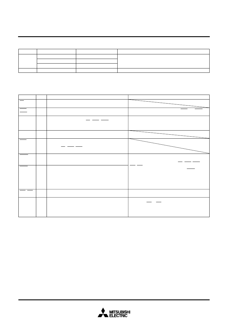
Signal
RD
BLW
BHW
ALE
φ
1
RDY
HOLD
HDLA
CS
0
–CS
3
BYTE
V
SS
V
CC
00
01
10
10
MD0
Processor mode bits
After reset is removed, the single-chip mode is selected. By chang-
ing the processor mode bits’ contents by software, the memory ex-
pansion mode or microprocessor mode can be selected.
Description
(Note 1)
Processor mode
Single-chip mode
Memory expansion mode
Microprocessor mode
Microprocessor mode
After reset is removed, the microprocessor mode is selected.
(Note 2)
Table 3. Selection method of processor mode
Table 4. Each bus control signal’s function
I/O
Output
Output
Output
Output
Input
Input
Output
Output
Input
Function
Read signal. Outputs “L” at read from the external area.
Write signal. Outputs “L” at write to the external area.
Address latch enable signal. Outputs “H” level pulse in the
period just before signals RD, BLW, BHW become “L”.
This is used to latch an address in an external circuit.
Internal standard clock’s output. Outputs system clock
(f
sys
).
Ready signal. The “L” level period of the last
φ
1
in the ac-
cess cycle for the external area (in other words, “L” level
period of RD, BLW, BHW) will be extended while “L” level
voltage is applied to this pin.
Hold request signal. Appliance of “L” level voltage will gen-
erate a hold request; appliance of “H” level voltage will re-
quest to terminate the hold state.
Hold acknowledge signal. Outputs “L” in the hold state.
Chip select signal. Outputs “L” in access to the specified
chip select area.
Input signal to select the external data bus width. When
this pin’s level = Vss, 16-bit width will be selected; and
when Vcc, 8-bit width will be selected.
Remarks
For operation differences between BLW and BHW de-
pending on the external data bus width, see Table 5.
In order to latch an address with signal ALE, do as follows:
While ALE = “H”, be sure to open a latch, so the address
will pass it.
While ALE = “L”, be sure to hold the address.
Acceptance and termination of a hold request is performed
at completion of the bus cycle while the BIU operates.
In the hold state, A
0
–A
23
, D
0
–D
15
, RD, BLW, BHW, ALE,
CS
0
–CS
3
enter the floating state. At termination of the hold
state, simultaneously with the timing when HLDA becomes
“H” level, the above floating state is terminated. Then, bus
access will be restarted 1 cycle of
φ
1
after.
In the hold state, also, the CPU operates with access to
the internal area. If the CPU accesses the external area, in
the hold state, the CPU stops its operation.
For details, refer to the section on the chip select wait con-
troller.
When BYTE = Vss level, by the register setting, each chip
select area (CS
1
to CS
3
) can have the 8-bit data bus, inde-
pendently.
For details, refer to the section on the chip select wait con-
troller.
Notes 1:
Processor mode bits = bits 0 and 1 of the processor mode register 0 (address 5E
16
)
2:
While the Vcc level voltage is applied to pin MD0, the processor mode bits are fixed to “10”.
相關(guān)PDF資料 |
PDF描述 |
|---|---|
| M37905F8CFP | 16-BIT CMOS MICROCOMPUTER |
| M37905F8CSP | 16-BIT CMOS MICROCOMPUTER |
| M37905M4C | DIODE SCHOTTKY DUAL COMMON-ANODE 25V 200mW 0.32V-vf 200mA-IFM 1mA-IF 2uA-IR SOT-323 3K/REEL |
| M37905M4C-XXXFP | 16 BIT CMOS MICROCOMPUTER |
| M37905M4C-XXXSP | 16 BIT CMOS MICROCOMPUTER |
相關(guān)代理商/技術(shù)參數(shù) |
參數(shù)描述 |
|---|---|
| M37903S4CHP | 制造商:RENESAS 制造商全稱:Renesas Technology Corp 功能描述:16-BIT CMOS MICROCOMPUTER |
| M37905F8CFP | 制造商:MITSUBISHI 制造商全稱:Mitsubishi Electric Semiconductor 功能描述:16-BIT CMOS MICROCOMPUTER |
| M37905F8CSP | 制造商:MITSUBISHI 制造商全稱:Mitsubishi Electric Semiconductor 功能描述:16-BIT CMOS MICROCOMPUTER |
| M37905M4C | 制造商:MITSUBISHI 制造商全稱:Mitsubishi Electric Semiconductor 功能描述:16 BIT CMOS MICROCOMPUTER |
| M37905M4C-XXXFP | 制造商:MITSUBISHI 制造商全稱:Mitsubishi Electric Semiconductor 功能描述:16 BIT CMOS MICROCOMPUTER |
發(fā)布緊急采購,3分鐘左右您將得到回復(fù)。