- 您現(xiàn)在的位置:買賣IC網(wǎng) > PDF目錄201303 > BX80532KC2800D (INTEL CORP) 32-BIT, 2800 MHz, MICROPROCESSOR PDF資料下載
參數(shù)資料
| 型號(hào): | BX80532KC2800D |
| 廠商: | INTEL CORP |
| 元件分類: | 微控制器/微處理器 |
| 英文描述: | 32-BIT, 2800 MHz, MICROPROCESSOR |
| 文件頁(yè)數(shù): | 57/129頁(yè) |
| 文件大小: | 1640K |
| 代理商: | BX80532KC2800D |
第1頁(yè)第2頁(yè)第3頁(yè)第4頁(yè)第5頁(yè)第6頁(yè)第7頁(yè)第8頁(yè)第9頁(yè)第10頁(yè)第11頁(yè)第12頁(yè)第13頁(yè)第14頁(yè)第15頁(yè)第16頁(yè)第17頁(yè)第18頁(yè)第19頁(yè)第20頁(yè)第21頁(yè)第22頁(yè)第23頁(yè)第24頁(yè)第25頁(yè)第26頁(yè)第27頁(yè)第28頁(yè)第29頁(yè)第30頁(yè)第31頁(yè)第32頁(yè)第33頁(yè)第34頁(yè)第35頁(yè)第36頁(yè)第37頁(yè)第38頁(yè)第39頁(yè)第40頁(yè)第41頁(yè)第42頁(yè)第43頁(yè)第44頁(yè)第45頁(yè)第46頁(yè)第47頁(yè)第48頁(yè)第49頁(yè)第50頁(yè)第51頁(yè)第52頁(yè)第53頁(yè)第54頁(yè)第55頁(yè)第56頁(yè)當(dāng)前第57頁(yè)第58頁(yè)第59頁(yè)第60頁(yè)第61頁(yè)第62頁(yè)第63頁(yè)第64頁(yè)第65頁(yè)第66頁(yè)第67頁(yè)第68頁(yè)第69頁(yè)第70頁(yè)第71頁(yè)第72頁(yè)第73頁(yè)第74頁(yè)第75頁(yè)第76頁(yè)第77頁(yè)第78頁(yè)第79頁(yè)第80頁(yè)第81頁(yè)第82頁(yè)第83頁(yè)第84頁(yè)第85頁(yè)第86頁(yè)第87頁(yè)第88頁(yè)第89頁(yè)第90頁(yè)第91頁(yè)第92頁(yè)第93頁(yè)第94頁(yè)第95頁(yè)第96頁(yè)第97頁(yè)第98頁(yè)第99頁(yè)第100頁(yè)第101頁(yè)第102頁(yè)第103頁(yè)第104頁(yè)第105頁(yè)第106頁(yè)第107頁(yè)第108頁(yè)第109頁(yè)第110頁(yè)第111頁(yè)第112頁(yè)第113頁(yè)第114頁(yè)第115頁(yè)第116頁(yè)第117頁(yè)第118頁(yè)第119頁(yè)第120頁(yè)第121頁(yè)第122頁(yè)第123頁(yè)第124頁(yè)第125頁(yè)第126頁(yè)第127頁(yè)第128頁(yè)第129頁(yè)
Intel Xeon Processor with 512 KB L2 Cache
Datasheet
33
2. The processor core clock frequency is derived from BCLK.
3. The period specified here is the average period. A given period may vary from this specification as governed
by the period stability specification (T2).
4. For the clock jitter specification, refer to the CK00 Clock Synthesizer/Driver Design Guidelines.
5. In this context, period stability is defined as the worst case timing difference between successive crossover
voltages. In other words, the largest absolute difference between adjacent clock periods must be less than
the period stability.
6. Slew rate is measured between the 35% and 65% points of the clock swing (VL and VH).
.
1. Unless otherwise noted, all specifications in this table apply to all processor frequencies and cache sizes.
2. Not 100% tested. Specified by design characterization.
3. All common clock AC timings for AGTL+ signals are referenced to the Crossing Voltage (VCROSS) of the
BCLK[1:0] at rising edge of BCLK0. All common clock AGTL+ signal timings are referenced at GTLREF at the
processor core.
4. Valid delay timings for these signals are specified into the test circuit described in Figure 5 and with GTLREF
at 2/3 * VCC ± 2%.
5. Specification is for a minimum swing defined between AGTL+ VIL_MAX to VIH_MIN. This assumes an edge rate
of 0.3 V/nS to 4.0 V/nS.
6. RESET# can be asserted (active) asynchronously, but must be deasserted synchronously.
7. This should be measured after V
CC and BCLK[1:0] become stable.
8. Maximum specification applies only while PWRGOOD is asserted.
.
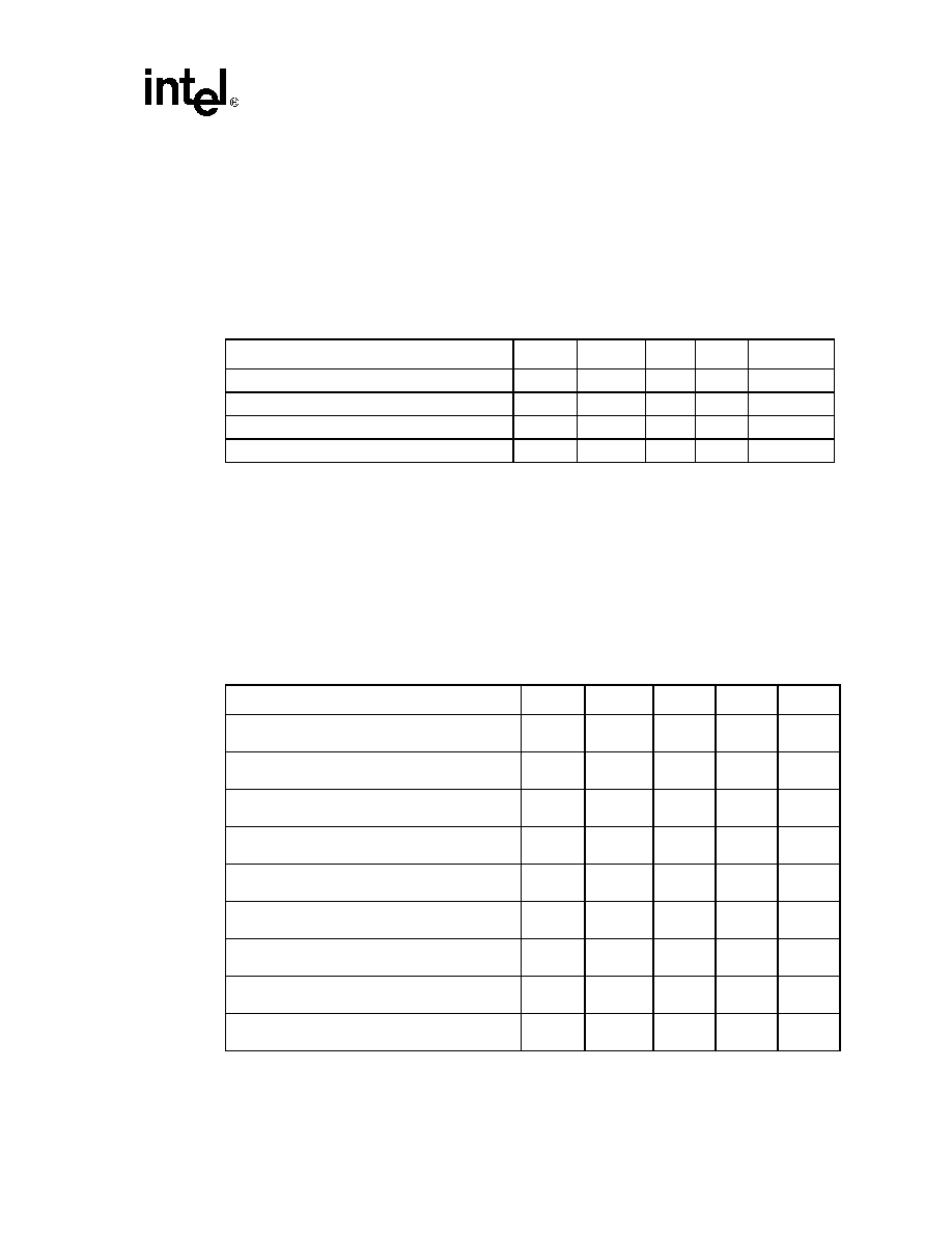
Table 15. Front Side Bus Common Clock AC Specifications
T# Parameter
Min
Max
Unit
Figure
Notes1, 2, 3
T10: Common Clock Output Valid Delay
0.12
1.27
nS
4
T11: Common Clock Input Setup Time
0.65
N/A
nS
5
T12: Common Clock Input Hold Time
0.40
N/A
nS
5
T13: RESET# Pulse Width
1.00
10.00
mS
6, 7, 8
Table 16. Front Side Bus Source Synchronous AC Specifications (Page 1 of 2)
T# Parameter
Min
Max
Unit
Figure
Notes
T20: Source Sync. Output Valid Delay (first data/
address only)
0.20
1.30
nS
1, 2, 3, 4,
5
T21: TVBD Source Sync. Data Output Valid Before
Data Strobe
0.85
nS
1, 2, 3, 4,
5, 8
T22: TVAD Source Sync. Data Output Valid After
Data Strobe
0.85
nS
1, 2, 3, 4,
5, 8
T23: TVBA Source Sync. Address Output Valid
Before Address Strobe
1.88
nS
1, 2, 3, 4,
5, 8
T24: TVAA Source Sync. Address Output Valid After
Address Strobe
1.88
nS
1, 2, 3, 4,
5, 9
T25: TSUSS Source Sync. Input Setup Time
0.21
nS
1, 2, 3, 4,
6
T26: THSS Source Sync. Input Hold Time
0.21
nS
1, 2, 3, 4,
6
T27: TSUCC Source Sync. Input Setup Time to
BCLK
0.65
nS
1, 2, 3, 4,
7
T28: TFASS First Address Strobe to Second Address
Strobe
1/2
BCLKs
1, 2, 3, 4,
10, 14
相關(guān)PDF資料 |
PDF描述 |
|---|---|
| BX80524R300128 | 32-BIT, 300 MHz, MICROPROCESSOR, XMA |
| BZV09/A0332/04 | 3A, 250VAC, FEMALE AND MALE, MAINS POWER CONNECTOR |
| BZV09/A0332/14 | 3A, 250VAC, FEMALE AND MALE, MAINS POWER CONNECTOR |
| BZV09/A0332/37 | 3A, 250VAC, FEMALE AND MALE, MAINS POWER CONNECTOR |
| BKT-146-01-F-V | 92 CONTACT(S), MALE, STRAIGHT TWO PART BOARD CONNECTOR, SURFACE MOUNT |
相關(guān)代理商/技術(shù)參數(shù) |
參數(shù)描述 |
|---|---|
| BX80532KC2800DU | 制造商:Intel 功能描述:MPU XEON PROCESSOR NETBURST 64-BIT 0.13UM 2.8GHZ - Boxed Product (Development Kits) |
| BX80532KC2800F | 制造商:Intel 功能描述:MPU XEON PROCESSOR NETBURST 64-BIT 0.13UM 2.8GHZ - Boxed Product (Development Kits) |
| BX80532KC3000D | 制造商:Intel 功能描述:MPU XEON PROCESSOR NETBURST 64-BIT 0.13UM 3GHZ - Boxed Product (Development Kits) |
| BX80532KC3000H | 制造商:Intel 功能描述:MPU XEON NETBURST 64-BIT 0.13UM 3GHZ - Boxed Product (Development Kits) |
| BX80532KE2000D | 制造商:Intel 功能描述:MPU XEON PROCESSOR NETBURST 64-BIT 0.13UM 2GHZ - Boxed Product (Development Kits) |
發(fā)布緊急采購(gòu),3分鐘左右您將得到回復(fù)。