- 您現(xiàn)在的位置:買賣IC網(wǎng) > PDF目錄201303 > BX80532KC2800D (INTEL CORP) 32-BIT, 2800 MHz, MICROPROCESSOR PDF資料下載
參數(shù)資料
| 型號: | BX80532KC2800D |
| 廠商: | INTEL CORP |
| 元件分類: | 微控制器/微處理器 |
| 英文描述: | 32-BIT, 2800 MHz, MICROPROCESSOR |
| 文件頁數(shù): | 116/129頁 |
| 文件大?。?/td> | 1640K |
| 代理商: | BX80532KC2800D |
第1頁第2頁第3頁第4頁第5頁第6頁第7頁第8頁第9頁第10頁第11頁第12頁第13頁第14頁第15頁第16頁第17頁第18頁第19頁第20頁第21頁第22頁第23頁第24頁第25頁第26頁第27頁第28頁第29頁第30頁第31頁第32頁第33頁第34頁第35頁第36頁第37頁第38頁第39頁第40頁第41頁第42頁第43頁第44頁第45頁第46頁第47頁第48頁第49頁第50頁第51頁第52頁第53頁第54頁第55頁第56頁第57頁第58頁第59頁第60頁第61頁第62頁第63頁第64頁第65頁第66頁第67頁第68頁第69頁第70頁第71頁第72頁第73頁第74頁第75頁第76頁第77頁第78頁第79頁第80頁第81頁第82頁第83頁第84頁第85頁第86頁第87頁第88頁第89頁第90頁第91頁第92頁第93頁第94頁第95頁第96頁第97頁第98頁第99頁第100頁第101頁第102頁第103頁第104頁第105頁第106頁第107頁第108頁第109頁第110頁第111頁第112頁第113頁第114頁第115頁當(dāng)前第116頁第117頁第118頁第119頁第120頁第121頁第122頁第123頁第124頁第125頁第126頁第127頁第128頁第129頁
Intel Xeon Processor with 512 KB L2 Cache
Datasheet
87
D[63:0]#
I/O
D[63:0]# (Data) are the data signals. These signals provide a 64-bit data path
between the processor front side bus agents, and must connect the appropriate
pins on all such agents. The data driver asserts DRDY# to indicate a valid data
transfer.
D[63:0]# are quad-pumped signals, and will thus be driven four times in a common
clock period. D[63:0]# are latched off the falling edge of both DSTBP[3:0]# and
DSTBN[3:0]#. Each group of 16 data signals correspond to a pair of one DSTBP#
and one DSTBN#. The following table shows the grouping of data signals to strobes
and DBI#.
Furthermore, the DBI# pins determine the polarity of the data signals. Each group
of 16 data signals corresponds to one DBI# signal. When the DBI# signal is active,
the corresponding data group is inverted and therefore sampled active high.
4
DBI[3:0]#
I/O
DBI[3:0]# are source synchronous and indicate the polarity of the D[63:0]# signals.
The DBI[3:0]# signals are activated when the data on the data bus is inverted. The
bus agent will invert the data bus signals if more than half the bits, within a 16-bit
group, change logic level in the next cycle.
4
DBSY#
I/O
DBSY# (Data Bus Busy) is asserted by the agent responsible for driving data on the
processor front side bus to indicate that the data bus is in use. The data bus is
released after DBSY# is deasserted. This signal must connect the appropriate pins
on all processor front side bus agents.
4
DEFER#
I
DEFER# is asserted by an agent to indicate that a transaction cannot be
guaranteed in-order completion. Assertion of DEFER# is normally the responsibility
of the addressed memory or I/O agent. This signal must connect the appropriate
pins of all processor front side bus agents.
4
DP[3:0]#
I/O
DP[3:0]# (Data Parity) provide parity protection for the D[63:0]# signals. They are
driven by the agent responsible for driving D[63:0]#, and must connect the
appropriate pins of all processor front side bus agents.
4
DRDY#
I/O
DRDY# (Data Ready) is asserted by the data driver on each data transfer,
indicating valid data on the data bus. In a multi-common clock data transfer, DRDY#
may be deasserted to insert idle clocks. This signal must connect the appropriate
pins of all processor front side bus agents.
4
DSTBN[3:0]#
I/O
Data strobe used to latch in D[63:0]#.
4
DSTBP[3:0]#
I/O
Data strobe used to latch in D[63:0]#.
4
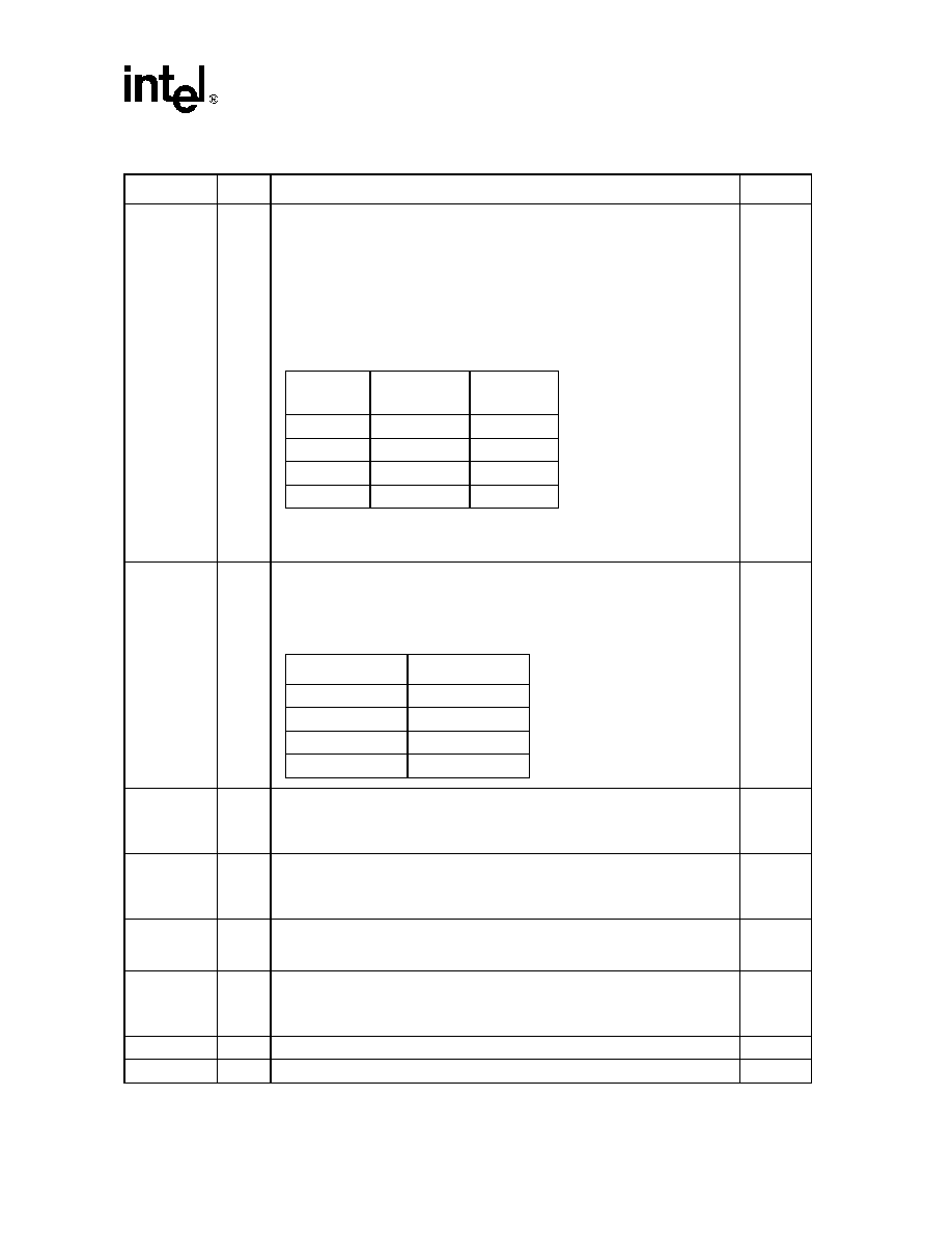
Table 41. Signal Definitions (Page 4 of 10)
Name
Type
Description
Notes
Data Group
DSTBN/
DSTBP
DBI#
D[15:0]#
0
D[31:16]#
1
D[47:32]#
2
D[63:48]#
3
DBI[3:0] Assignment To Data Bus
Bus Signal
Data Bus Signals
DBI0#
D[15:0]#
DBI1#
D[31:16]#
DBI2#
D[47:32]#
DBI3#
D[63:48]#
相關(guān)PDF資料 |
PDF描述 |
|---|---|
| BX80524R300128 | 32-BIT, 300 MHz, MICROPROCESSOR, XMA |
| BZV09/A0332/04 | 3A, 250VAC, FEMALE AND MALE, MAINS POWER CONNECTOR |
| BZV09/A0332/14 | 3A, 250VAC, FEMALE AND MALE, MAINS POWER CONNECTOR |
| BZV09/A0332/37 | 3A, 250VAC, FEMALE AND MALE, MAINS POWER CONNECTOR |
| BKT-146-01-F-V | 92 CONTACT(S), MALE, STRAIGHT TWO PART BOARD CONNECTOR, SURFACE MOUNT |
相關(guān)代理商/技術(shù)參數(shù) |
參數(shù)描述 |
|---|---|
| BX80532KC2800DU | 制造商:Intel 功能描述:MPU XEON PROCESSOR NETBURST 64-BIT 0.13UM 2.8GHZ - Boxed Product (Development Kits) |
| BX80532KC2800F | 制造商:Intel 功能描述:MPU XEON PROCESSOR NETBURST 64-BIT 0.13UM 2.8GHZ - Boxed Product (Development Kits) |
| BX80532KC3000D | 制造商:Intel 功能描述:MPU XEON PROCESSOR NETBURST 64-BIT 0.13UM 3GHZ - Boxed Product (Development Kits) |
| BX80532KC3000H | 制造商:Intel 功能描述:MPU XEON NETBURST 64-BIT 0.13UM 3GHZ - Boxed Product (Development Kits) |
| BX80532KE2000D | 制造商:Intel 功能描述:MPU XEON PROCESSOR NETBURST 64-BIT 0.13UM 2GHZ - Boxed Product (Development Kits) |
發(fā)布緊急采購,3分鐘左右您將得到回復(fù)。