- 您現(xiàn)在的位置:買賣IC網(wǎng) > PDF目錄201303 > BX80532KC2800D (INTEL CORP) 32-BIT, 2800 MHz, MICROPROCESSOR PDF資料下載
參數(shù)資料
| 型號: | BX80532KC2800D |
| 廠商: | INTEL CORP |
| 元件分類: | 微控制器/微處理器 |
| 英文描述: | 32-BIT, 2800 MHz, MICROPROCESSOR |
| 文件頁數(shù): | 47/129頁 |
| 文件大小: | 1640K |
| 代理商: | BX80532KC2800D |
第1頁第2頁第3頁第4頁第5頁第6頁第7頁第8頁第9頁第10頁第11頁第12頁第13頁第14頁第15頁第16頁第17頁第18頁第19頁第20頁第21頁第22頁第23頁第24頁第25頁第26頁第27頁第28頁第29頁第30頁第31頁第32頁第33頁第34頁第35頁第36頁第37頁第38頁第39頁第40頁第41頁第42頁第43頁第44頁第45頁第46頁當(dāng)前第47頁第48頁第49頁第50頁第51頁第52頁第53頁第54頁第55頁第56頁第57頁第58頁第59頁第60頁第61頁第62頁第63頁第64頁第65頁第66頁第67頁第68頁第69頁第70頁第71頁第72頁第73頁第74頁第75頁第76頁第77頁第78頁第79頁第80頁第81頁第82頁第83頁第84頁第85頁第86頁第87頁第88頁第89頁第90頁第91頁第92頁第93頁第94頁第95頁第96頁第97頁第98頁第99頁第100頁第101頁第102頁第103頁第104頁第105頁第106頁第107頁第108頁第109頁第110頁第111頁第112頁第113頁第114頁第115頁第116頁第117頁第118頁第119頁第120頁第121頁第122頁第123頁第124頁第125頁第126頁第127頁第128頁第129頁
Intel Xeon Processor with 512 KB L2 Cache
24
Datasheet
9. SM_Vcc is required for correct VID logic operation of the Intel Xeon processor with 512 KB L2 cache.
Refer to Figure 19 for details.
2.9
Asynchronous GTL+ Signals
The Intel
Xeon processor with 512 KB L2 cache does not utilize CMOS voltage levels on any
signals that connect to the processor silicon. As a result, legacy input signals such as A20M#,
IGNNE#, INIT#, LINT0/INTR, LINT1/NMI, SMI#, SLP#, and STPCLK# utilize GTL+ input
buffers. Legacy output FERR#/PBE# and other non-AGTL+ signals IERR#, THERMTRIP# and
PROCHOT# utilize GTL+ output buffers. All of these asynchronous GTL+ signals follow the same
DC requirements as AGTL+ signals, however the outputs are not driven high (during the logical 0-
to-1 transition) by the processor (the major difference between GTL+ and AGTL+). Asynchronous
GTL+ signals do not have setup or hold time specifications in relation to BCLK[1:0]. However, all
of the asynchronous GTL+ signals are required to be asserted for at least two BCLKs in order for
the asynchronous GTL+ signal groups.
SMBus signals are derived from components mounted on the processor interposer along with the
details.
2.10
Maximum Ratings
Table 5 lists the processor’s maximum environmental stress ratings. Functional operation at the
absolute maximum and minimum is neither implied nor guaranteed. The processor should not
receive a clock while subjected to these conditions. Functional operating parameters are listed in
the AC and DC tables. Extended exposure to the maximum ratings may affect device reliability.
Furthermore, although the processor contains protective circuitry to resist damage from static
electric discharge, one should always take precautions to avoid high static voltages or electric
fields.
1. This rating applies to any pin of the processor.
2. Contact Intel for storage requirements in excess of one year.
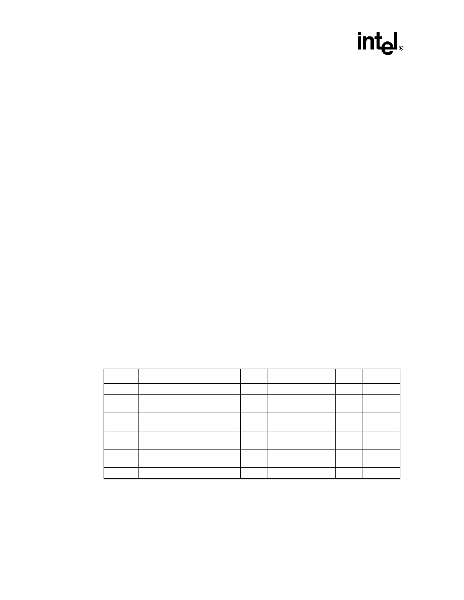
Table 5. Processor Absolute Maximum Ratings
Symbol
Parameter
Min
Max
Unit
Notes
T
STORAGE
Processor storage temperature
-40
85
°C
2
V
CC
Any processor supply voltage with
respect to VSS
-0.3
1.75
V
1
V
inAGTL+
AGTL+ buffer DC input voltage with
respect to VSS
-0.1
1.75
V
inGTL+
Async GTL+ buffer DC input voltage
with respect to Vss
-0.1
1.75
V
inSMBus
SMBus buffer DC input voltage with
respect to Vss
-0.3
6.0
V
I
VID
Max VID pin current
5
mA
相關(guān)PDF資料 |
PDF描述 |
|---|---|
| BX80524R300128 | 32-BIT, 300 MHz, MICROPROCESSOR, XMA |
| BZV09/A0332/04 | 3A, 250VAC, FEMALE AND MALE, MAINS POWER CONNECTOR |
| BZV09/A0332/14 | 3A, 250VAC, FEMALE AND MALE, MAINS POWER CONNECTOR |
| BZV09/A0332/37 | 3A, 250VAC, FEMALE AND MALE, MAINS POWER CONNECTOR |
| BKT-146-01-F-V | 92 CONTACT(S), MALE, STRAIGHT TWO PART BOARD CONNECTOR, SURFACE MOUNT |
相關(guān)代理商/技術(shù)參數(shù) |
參數(shù)描述 |
|---|---|
| BX80532KC2800DU | 制造商:Intel 功能描述:MPU XEON PROCESSOR NETBURST 64-BIT 0.13UM 2.8GHZ - Boxed Product (Development Kits) |
| BX80532KC2800F | 制造商:Intel 功能描述:MPU XEON PROCESSOR NETBURST 64-BIT 0.13UM 2.8GHZ - Boxed Product (Development Kits) |
| BX80532KC3000D | 制造商:Intel 功能描述:MPU XEON PROCESSOR NETBURST 64-BIT 0.13UM 3GHZ - Boxed Product (Development Kits) |
| BX80532KC3000H | 制造商:Intel 功能描述:MPU XEON NETBURST 64-BIT 0.13UM 3GHZ - Boxed Product (Development Kits) |
| BX80532KE2000D | 制造商:Intel 功能描述:MPU XEON PROCESSOR NETBURST 64-BIT 0.13UM 2GHZ - Boxed Product (Development Kits) |
發(fā)布緊急采購,3分鐘左右您將得到回復(fù)。