- 您現(xiàn)在的位置:買賣IC網(wǎng) > PDF目錄201303 > BX80532KC2800D (INTEL CORP) 32-BIT, 2800 MHz, MICROPROCESSOR PDF資料下載
參數(shù)資料
| 型號(hào): | BX80532KC2800D |
| 廠商: | INTEL CORP |
| 元件分類: | 微控制器/微處理器 |
| 英文描述: | 32-BIT, 2800 MHz, MICROPROCESSOR |
| 文件頁(yè)數(shù): | 46/129頁(yè) |
| 文件大?。?/td> | 1640K |
| 代理商: | BX80532KC2800D |
第1頁(yè)第2頁(yè)第3頁(yè)第4頁(yè)第5頁(yè)第6頁(yè)第7頁(yè)第8頁(yè)第9頁(yè)第10頁(yè)第11頁(yè)第12頁(yè)第13頁(yè)第14頁(yè)第15頁(yè)第16頁(yè)第17頁(yè)第18頁(yè)第19頁(yè)第20頁(yè)第21頁(yè)第22頁(yè)第23頁(yè)第24頁(yè)第25頁(yè)第26頁(yè)第27頁(yè)第28頁(yè)第29頁(yè)第30頁(yè)第31頁(yè)第32頁(yè)第33頁(yè)第34頁(yè)第35頁(yè)第36頁(yè)第37頁(yè)第38頁(yè)第39頁(yè)第40頁(yè)第41頁(yè)第42頁(yè)第43頁(yè)第44頁(yè)第45頁(yè)當(dāng)前第46頁(yè)第47頁(yè)第48頁(yè)第49頁(yè)第50頁(yè)第51頁(yè)第52頁(yè)第53頁(yè)第54頁(yè)第55頁(yè)第56頁(yè)第57頁(yè)第58頁(yè)第59頁(yè)第60頁(yè)第61頁(yè)第62頁(yè)第63頁(yè)第64頁(yè)第65頁(yè)第66頁(yè)第67頁(yè)第68頁(yè)第69頁(yè)第70頁(yè)第71頁(yè)第72頁(yè)第73頁(yè)第74頁(yè)第75頁(yè)第76頁(yè)第77頁(yè)第78頁(yè)第79頁(yè)第80頁(yè)第81頁(yè)第82頁(yè)第83頁(yè)第84頁(yè)第85頁(yè)第86頁(yè)第87頁(yè)第88頁(yè)第89頁(yè)第90頁(yè)第91頁(yè)第92頁(yè)第93頁(yè)第94頁(yè)第95頁(yè)第96頁(yè)第97頁(yè)第98頁(yè)第99頁(yè)第100頁(yè)第101頁(yè)第102頁(yè)第103頁(yè)第104頁(yè)第105頁(yè)第106頁(yè)第107頁(yè)第108頁(yè)第109頁(yè)第110頁(yè)第111頁(yè)第112頁(yè)第113頁(yè)第114頁(yè)第115頁(yè)第116頁(yè)第117頁(yè)第118頁(yè)第119頁(yè)第120頁(yè)第121頁(yè)第122頁(yè)第123頁(yè)第124頁(yè)第125頁(yè)第126頁(yè)第127頁(yè)第128頁(yè)第129頁(yè)
Intel Xeon Processor with 512 KB L2 Cache
Datasheet
23
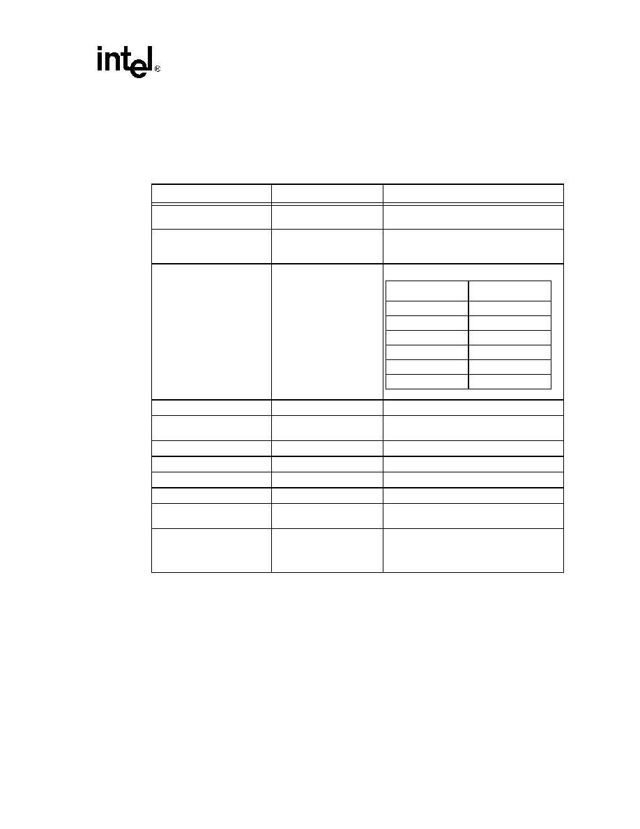
rising edge of BCLK0. Asynchronous signals are still present (A20M#, IGNNE#, etc.) and can
become active at any time during the clock cycle. Table 4 identifies which signals are common
clock, source synchronous and asynchronous.
1. Refer to Section 5.2 for signal descriptions.
2. These signal groups are not terminated by the processor. Refer the ITP700 Debug Port Design Guide and
corresponding Design Guide for termination requirements and further details.
3. The Intel Xeon processor with 512 KB L2 cache utilizes only BR0# and BR1#. BR2# and BR3# are not
driven by the processor but must be terminated to V
CC. For additional details regarding the BR[3:0]# signals,
see Section 5.2 and Section 7.1 and the appropriate Platform Design Guidelines.
4. These signals do not have on-die termination. Refer to corresponding Platform Design Guidelines for
termination requirements.
5. Note that Reset initialization function of these pins is now a software function on the Intel Xeon
processor with 512 KB L2 cache.
6. The value of these pins during the active-to-inactive edge of RESET# to determine processor configuration
options. See Section 7.1 for details.
7. These signals may be driven simultaneously by multiple agents (wired-or).
8. These signals are not terminated by the processor’s on-die termination. However, some signals in this group
include termination on the processor interposer. See Section 7.4 for details.
Table 4. Front Side Bus Signal Groups
Signal Group
Type
Signals 1
AGTL+ Common Clock Input
Synchronous to BCLK[1:0]
BPRI#, BR[3:1]#3,4, DEFER#, RESET#4,
RS[2:0]#, RSP#, TRDY#
AGTL+ Common Clock I/O
Synchronous to BCLK[1:0]
ADS#, AP[1:0]#, BINIT#7, BNR#7,
BPM[5:0]#2, BR0#2, DBSY#, DP[3:0]#,
DRDY#, HIT#7, HITM#7, LOCK#, MCERR#7
AGTL+ Source Synchronous
I/O
Synchronous to assoc.
strobe
AGTL+ Strobes
Synchronous to BCLK[1:0]
ADSTB[1:0]#, DSTBP[3:0]#, DSTBN[3:0]#
Asynchronous GTL+ Input 4
Asynchronous
A20M#5, IGNNE#5, INIT#6, LINT0/INTR5,
LINT1/NMI5, SMI#6, SLP#, STPCLK#
Asynchronous GTL+ Output 4
Asynchronous
FERR#, IERR#, THERMTRIP#, PROCHOT#
Front Side Bus Clock
Clock
BCLK1, BCLK0
TAP Input 2
Synchronous to TCK
TCK, TDI, TMS, TRST#
TAP Output 2
Synchronous to TCK
TDO
SMBus Interface 8
Synchronous to SM_CLK
SM_EP_A[2:0], SM_TS_A[1:0], SM_DAT,
SM_CLK, SM_ALERT#, SM_WP
Power/Other
BSEL[1:0], COMP[1:0], GTLREF, ODTEN,
Reserved, SKTOCC#, TESTHI[6:0],VID[4:0],
VCC, SM_VCC
9, V
CCA, VCCIOPLL, VSSA, VSS,
VCCSENSE, VSSSENSE, PWRGOOD
Signals
Associated Strobe
REQ[4:0]#,A[16:3]#6
ADSTB0#
A[35:17]#5
ADSTB1#
D[15:0]#, DBI0#
DSTBP0#, DSTBN0#
D[31:16]#, DBI1#
DSTBP1#, DSTBN1#
D[47:32]#, DBI2#
DSTBP2#, DSTBN2#
D[63:48]#, DBI3#
DSTBP3#, DSTBN3#
相關(guān)PDF資料 |
PDF描述 |
|---|---|
| BX80524R300128 | 32-BIT, 300 MHz, MICROPROCESSOR, XMA |
| BZV09/A0332/04 | 3A, 250VAC, FEMALE AND MALE, MAINS POWER CONNECTOR |
| BZV09/A0332/14 | 3A, 250VAC, FEMALE AND MALE, MAINS POWER CONNECTOR |
| BZV09/A0332/37 | 3A, 250VAC, FEMALE AND MALE, MAINS POWER CONNECTOR |
| BKT-146-01-F-V | 92 CONTACT(S), MALE, STRAIGHT TWO PART BOARD CONNECTOR, SURFACE MOUNT |
相關(guān)代理商/技術(shù)參數(shù) |
參數(shù)描述 |
|---|---|
| BX80532KC2800DU | 制造商:Intel 功能描述:MPU XEON PROCESSOR NETBURST 64-BIT 0.13UM 2.8GHZ - Boxed Product (Development Kits) |
| BX80532KC2800F | 制造商:Intel 功能描述:MPU XEON PROCESSOR NETBURST 64-BIT 0.13UM 2.8GHZ - Boxed Product (Development Kits) |
| BX80532KC3000D | 制造商:Intel 功能描述:MPU XEON PROCESSOR NETBURST 64-BIT 0.13UM 3GHZ - Boxed Product (Development Kits) |
| BX80532KC3000H | 制造商:Intel 功能描述:MPU XEON NETBURST 64-BIT 0.13UM 3GHZ - Boxed Product (Development Kits) |
| BX80532KE2000D | 制造商:Intel 功能描述:MPU XEON PROCESSOR NETBURST 64-BIT 0.13UM 2GHZ - Boxed Product (Development Kits) |
發(fā)布緊急采購(gòu),3分鐘左右您將得到回復(fù)。