- 您現(xiàn)在的位置:買賣IC網(wǎng) > PDF目錄383982 > UPD703130GC-8EU (NEC Corp.) MOS INTEGRATED CIRCUIT PDF資料下載
參數(shù)資料
| 型號: | UPD703130GC-8EU |
| 廠商: | NEC Corp. |
| 英文描述: | MOS INTEGRATED CIRCUIT |
| 中文描述: | 馬鞍山集成電路 |
| 文件頁數(shù): | 55/72頁 |
| 文件大小: | 601K |
| 代理商: | UPD703130GC-8EU |
第1頁第2頁第3頁第4頁第5頁第6頁第7頁第8頁第9頁第10頁第11頁第12頁第13頁第14頁第15頁第16頁第17頁第18頁第19頁第20頁第21頁第22頁第23頁第24頁第25頁第26頁第27頁第28頁第29頁第30頁第31頁第32頁第33頁第34頁第35頁第36頁第37頁第38頁第39頁第40頁第41頁第42頁第43頁第44頁第45頁第46頁第47頁第48頁第49頁第50頁第51頁第52頁第53頁第54頁當前第55頁第56頁第57頁第58頁第59頁第60頁第61頁第62頁第63頁第64頁第65頁第66頁第67頁第68頁第69頁第70頁第71頁第72頁
Preliminary Data Sheet U15390EJ1V0DS
55
μ
PD703130
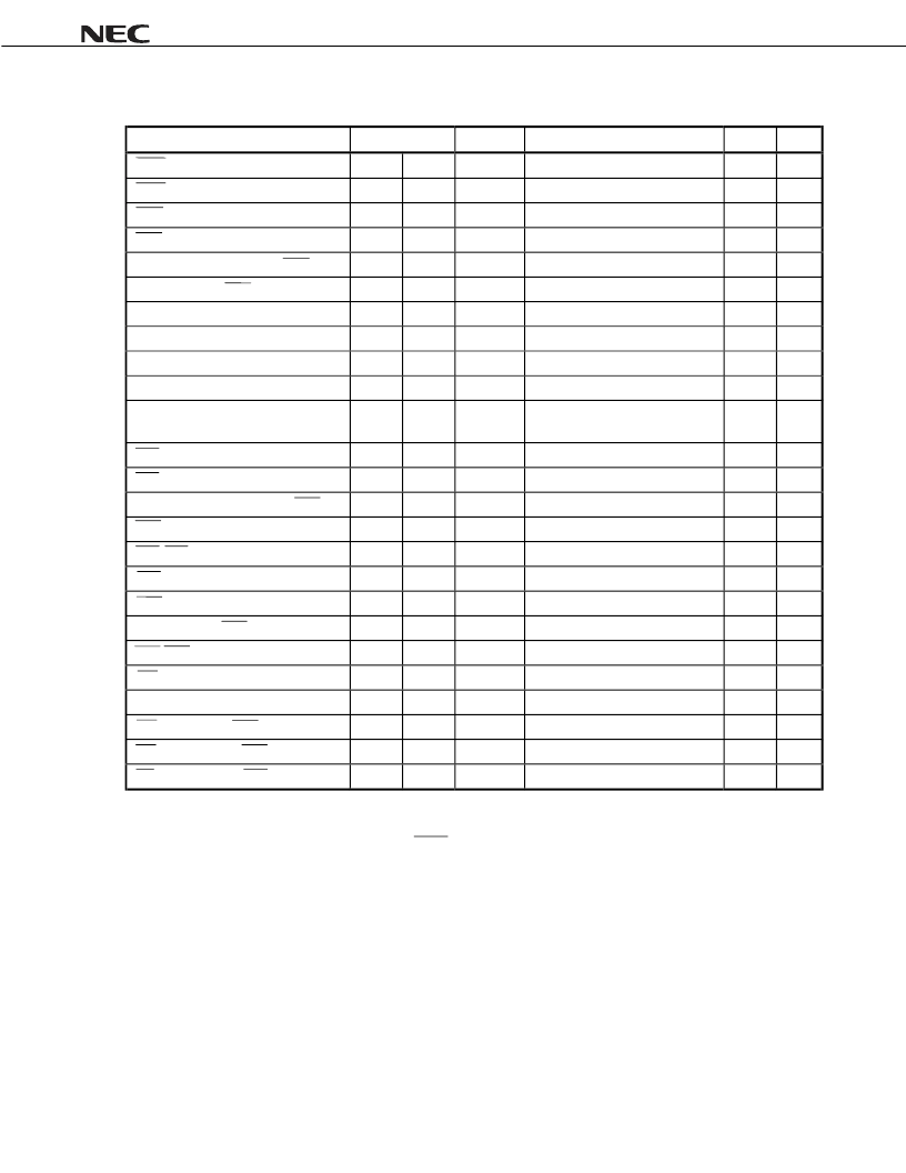
(h) DMA flyby transfer timing (external I/O
→
DRAM (EDO, high-speed page) transfer) (1/3)
Parameter
Symbol
Condition
MIN.
MAX.
Unit
WAIT setup time (to CLKOUT
↓
)
<24>
t
SWK
15
ns
WAIT hold time (from CLKOUT
↓
)
<25>
t
HKW
2
ns
IORD low-level width
<32>
t
WRDL
(2 + w
RH
+ w
DA
+ w
F
+ w)T – 10
ns
IORD high-level width
<33>
t
WRDH
T – 10
ns
Delay time from address to IORD
↑
<34>
t
DARD
0.5T – 10
ns
Delay time from IORD
↑
to address
<35>
t
DRDA
(0.5 + i)T – 10
ns
Row address setup time
<56>
t
ASR
(0.5 + w
RP
)T – 10
ns
Row address hold time
<57>
t
RAH
(0.5 + w
RH
)T – 10
ns
Column address setup time
<58>
t
ASC
0.5T – 10
ns
Column address hold time
<59>
t
CAH
(1.5 + w
DA
+ w
F
)T – 10
ns
Read/write cycle time
<60>
t
RC
(3 + w
RP
+ w
RH
+ w
DA
+ w
F
+ w)T
– 10
ns
RAS precharge time
<61>
t
RP
(0.5 + w
RP
)T – 10
ns
RAS hold time
<63>
t
RSH
(1.5 + w
DA
+ w
F
)T – 10
ns
Column address read time for RAS
<64>
t
RAL
(2 + w
CP
+ w
DA
+ w
F
+ w)T – 10
ns
CAS pulse width
<65>
t
CAS
(1 + w
DA
+ w
F
)T – 10
ns
CAS-RAS precharge time
<66>
t
CRP
(1 + w
RP
)T – 10
ns
CAS hold time
<67>
t
CSH
(2 + w
RH
+ w
DA
+ w
F
+ w)T – 10
ns
CAS precharge time
<71>
t
CPN
(2 + w
RP
+ w
RH
+ w)T – 10
ns
Delay time from RAS to column address
<76>
t
RAD
(0.5 + w
RH
)T – 10
ns
RAS-CAS delay time
<77>
t
RCD
(1 + w
RH
+ w)T – 10
ns
CAS precharge time
<81>
t
CP
(0.5 + w
CP
+ w)T – 10
ns
High-speed page mode cycle time
<82>
t
PC
(2 + w
CP
+ w
DA
+ w
F
+ w)T – 10
ns
RAS hold time for CAS precharge
<83>
t
RHCP
(2.5 + w
CP
+ w
DA
+ w)T – 10
ns
WE hold time (from CAS
↓
)
<85>
t
WCH
(1 + w
DA
)T – 10
ns
WE read time (from RAS
↑
)
<88>
t
RWL
w
CP
= 0
(1.5 + w
DA
+ w)T – 10
ns
Remarks 1.
T = t
CYK
2.
w: The number of waits due to WAIT.
3.
w
RH
: The number of waits due to the RHCxx bit of the DRCn register (n = 0 to 3, xx = 00 to 03, 10 to
13).
4.
w
DA
: The number of waits due to the DACxx bit of the DRCn register (n = 0 to 3, xx = 00 to 03, 10 to
13).
5.
w
RP
: The number of waits due to the RPCxx bit of the DRCn register (n = 0 to 3, xx = 00 to 03, 10 to
13).
6.
w
CP
: The number of waits due to the CPCxx bit of the DRCn register (n = 0 to 3, xx = 00 to 03, 10 to
13).
7.
w
F
: The number of waits that are inserted for a source-side access during a DMA flyby transfer.
8.
i: The number of idle states that are inserted when a write cycle follows a read cycle.
相關PDF資料 |
PDF描述 |
|---|---|
| UPD703130 | MOS INTEGRATED CIRCUIT |
| UPD703201 | 32-BIT SINGLE-CHIP MICROCONTROLLERS |
| UPD703204 | 32-BIT SINGLE-CHIP MICROCONTROLLERS |
| UPD70F30025AGC-25 | LJT 24C 12#16 12#12 PIN PLUG |
| UPD70F3004AGC-33 | 32-bit RISC Microcontrollers |
相關代理商/技術參數(shù) |
參數(shù)描述 |
|---|---|
| UPD703131A | 制造商:NEC 制造商全稱:NEC 功能描述:32-Bit Single-Chip Microcontrollers |
| UPD703131AF1-EN4 | 制造商:NEC 制造商全稱:NEC 功能描述:32-Bit Single-Chip Microcontrollers |
| UPD703131AF1-XXX-EN4 | 制造商:NEC 制造商全稱:NEC 功能描述:32-Bit Single-Chip Microcontrollers |
| UPD703131AGJ-XXX-UEN | 制造商:NEC 制造商全稱:NEC 功能描述:32-Bit Single-Chip Microcontrollers |
| UPD703131AY | 制造商:NEC 制造商全稱:NEC 功能描述:32-Bit Single-Chip Microcontrollers |
發(fā)布緊急采購,3分鐘左右您將得到回復。