- 您現(xiàn)在的位置:買(mǎi)賣(mài)IC網(wǎng) > PDF目錄383723 > OR3LP26B Field-Programmable System Chip (FPSC) Embedded Master/Target PCI Interface PDF資料下載
參數(shù)資料
| 型號(hào): | OR3LP26B |
| 英文描述: | Field-Programmable System Chip (FPSC) Embedded Master/Target PCI Interface |
| 中文描述: | 現(xiàn)場(chǎng)可編程系統(tǒng)芯片(促進(jìn)文化基金)嵌入式主/目標(biāo)PCI接口 |
| 文件頁(yè)數(shù): | 32/184頁(yè) |
| 文件大小: | 5590K |
| 代理商: | OR3LP26B |
第1頁(yè)第2頁(yè)第3頁(yè)第4頁(yè)第5頁(yè)第6頁(yè)第7頁(yè)第8頁(yè)第9頁(yè)第10頁(yè)第11頁(yè)第12頁(yè)第13頁(yè)第14頁(yè)第15頁(yè)第16頁(yè)第17頁(yè)第18頁(yè)第19頁(yè)第20頁(yè)第21頁(yè)第22頁(yè)第23頁(yè)第24頁(yè)第25頁(yè)第26頁(yè)第27頁(yè)第28頁(yè)第29頁(yè)第30頁(yè)第31頁(yè)當(dāng)前第32頁(yè)第33頁(yè)第34頁(yè)第35頁(yè)第36頁(yè)第37頁(yè)第38頁(yè)第39頁(yè)第40頁(yè)第41頁(yè)第42頁(yè)第43頁(yè)第44頁(yè)第45頁(yè)第46頁(yè)第47頁(yè)第48頁(yè)第49頁(yè)第50頁(yè)第51頁(yè)第52頁(yè)第53頁(yè)第54頁(yè)第55頁(yè)第56頁(yè)第57頁(yè)第58頁(yè)第59頁(yè)第60頁(yè)第61頁(yè)第62頁(yè)第63頁(yè)第64頁(yè)第65頁(yè)第66頁(yè)第67頁(yè)第68頁(yè)第69頁(yè)第70頁(yè)第71頁(yè)第72頁(yè)第73頁(yè)第74頁(yè)第75頁(yè)第76頁(yè)第77頁(yè)第78頁(yè)第79頁(yè)第80頁(yè)第81頁(yè)第82頁(yè)第83頁(yè)第84頁(yè)第85頁(yè)第86頁(yè)第87頁(yè)第88頁(yè)第89頁(yè)第90頁(yè)第91頁(yè)第92頁(yè)第93頁(yè)第94頁(yè)第95頁(yè)第96頁(yè)第97頁(yè)第98頁(yè)第99頁(yè)第100頁(yè)第101頁(yè)第102頁(yè)第103頁(yè)第104頁(yè)第105頁(yè)第106頁(yè)第107頁(yè)第108頁(yè)第109頁(yè)第110頁(yè)第111頁(yè)第112頁(yè)第113頁(yè)第114頁(yè)第115頁(yè)第116頁(yè)第117頁(yè)第118頁(yè)第119頁(yè)第120頁(yè)第121頁(yè)第122頁(yè)第123頁(yè)第124頁(yè)第125頁(yè)第126頁(yè)第127頁(yè)第128頁(yè)第129頁(yè)第130頁(yè)第131頁(yè)第132頁(yè)第133頁(yè)第134頁(yè)第135頁(yè)第136頁(yè)第137頁(yè)第138頁(yè)第139頁(yè)第140頁(yè)第141頁(yè)第142頁(yè)第143頁(yè)第144頁(yè)第145頁(yè)第146頁(yè)第147頁(yè)第148頁(yè)第149頁(yè)第150頁(yè)第151頁(yè)第152頁(yè)第153頁(yè)第154頁(yè)第155頁(yè)第156頁(yè)第157頁(yè)第158頁(yè)第159頁(yè)第160頁(yè)第161頁(yè)第162頁(yè)第163頁(yè)第164頁(yè)第165頁(yè)第166頁(yè)第167頁(yè)第168頁(yè)第169頁(yè)第170頁(yè)第171頁(yè)第172頁(yè)第173頁(yè)第174頁(yè)第175頁(yè)第176頁(yè)第177頁(yè)第178頁(yè)第179頁(yè)第180頁(yè)第181頁(yè)第182頁(yè)第183頁(yè)第184頁(yè)
ORCAOR3LP26B FPSC
Embedded Master/Target PCI Interface
Data Sheet
March 2000
32
L Lucent Technologies Inc.
PCI Bus Core Detailed Description
Dual Port
(continued)
Embedded Core Bit Stream Configurable Options
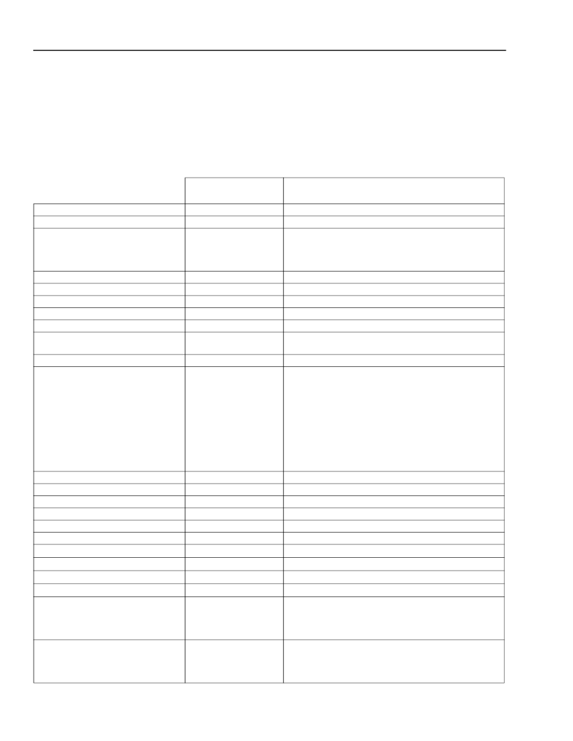
Table 12 lists all optional functionality in the PCI core that can be defined via bits in the FPGA configuration RAM.
The table also lists the settings available for each feature. Each of these options is configured using the FPSC
Design Kit software.
Table 12. PCI Core Options Settable via FPGA Configuration RAM Bits
Address in
Configuration Space
08
09—0B
Command register bit 2
Optional Settings
Revision ID
Class Code
Bus Master Support
Any 8-bit value.
Any 24-bit value.
Four options.
I
Initially disabled, read-only.
I
Initially disabled, read/write.
I
Initially enabled, read-only.
Include or exclude in decode for
pci_mcfg_stat
.
Include or exclude in decode for
pci_tcfg_stat
.
Include or exclude in decode for
pci_mcfg_stat
.
Include or exclude in decode for
pci_mcfg_stat
.
Include or exclude in decode for
pci_tcfg_stat
.
Include or exclude in decode for
pci_tcfg_stat
.
Report: Data Parity Error Detected
Report: Target Abort Signaled
Report: Target Abort Received
Report: Master Abort Received
Report: System Error Signaled
Report: Parity Error Detected
(nonmaskable)
Latency Timer Initial Value
Base Address Register (BAR) Area 1
Status register bit 8
Status register bit 11
Status register bit 12
Status register bit 13
Status register bit 14
Status register bit 15
OD
Any 8-bit value divisible by 8.
I
One or two 32-bit BARs or one 64-bit BAR, or none
(i.e., unprogrammed).
I
If 64-bit BAR, must be memory; page size can be from
2
4
to 2
64
bytes.
I
32-bit BARs can be memory or I/O.
I
If 32-bit I/O BAR, page size can be from 2
2
to 2
32
bytes.
I
If 32-bit memory BAR, address space can be 2
20
or 2
32
bytes, page size can be 2
4
to the maximum (2
20
or 2
32
)
bytes.
I
If memory, can be prefetchable or nonprefetchable.
Same as for BAR area 1.
Same as for BAR area 1.
Any 16-bit value.
Any 16-bit value.
Any 8-bit value.
Any 8-bit value.
Dual port or quad port.
Fast or slew-limited PCI output buffers.
fclk1
or
fclk2
.
fclk1
or
fclk2
.
Enabled or disabled; when enabled, PCI core will not
transfer most significant byte(s) of Target address if they
match previous Target operation's address and require
additional bus cycle(s).
Normal (16) or extended (32); note that only normal
latency complies with PCI Specification. Extended latency
may be specified in proprietary systems where bandwidth
requirements override fairness considerations.
10—17
Base Address Register (BAR) Area 2
Base Address Register (BAR) Area 3
Subsystem Vendor ID
Subsystem ID
Minimum Grant (Min_Gnt)
Maximum Latency (Max_Lat)
Port Mode
I/O Mode
Master FIFO Interface Clock
Target FIFO Interface Clock
Target Address Comparator
18—1F
20—27
2C—2D
2E—2F
3E
3F
—
—
—
—
—
Target Maximum Intial Latency
—
相關(guān)PDF資料 |
PDF描述 |
|---|---|
| OR3TP12-6BA256 | Single 2.3V 10 MHz OP w/ CS, I temp, -40C to +85C, 8-TSSOP, T/R |
| OR3TP12-6BA256I | Single 2.3V 10 MHZ OP, -40C to +125C, 14-SOIC 150mil, TUBE |
| OR3TP12-6BA352 | Quad 2.3V 10 MHz OP, I temp, -40C to +85C, 14-PDIP, TUBE |
| OR3TP12-6BA352I | Quad 2.3V 10 MHz OP, I temp, -40C to +85C, 14-TSSOP, TUBE |
| OR3TP12-6PS240 | Single 2.3V 10 MHZ OP, -40C to +125C, 14-SOIC 150mil, T/R |
相關(guān)代理商/技術(shù)參數(shù) |
參數(shù)描述 |
|---|---|
| OR3LP26BBA352-DB | 功能描述:FPGA - 現(xiàn)場(chǎng)可編程門(mén)陣列 FPSC PCI INTERFACE RoHS:否 制造商:Altera Corporation 系列:Cyclone V E 柵極數(shù)量: 邏輯塊數(shù)量:943 內(nèi)嵌式塊RAM - EBR:1956 kbit 輸入/輸出端數(shù)量:128 最大工作頻率:800 MHz 工作電源電壓:1.1 V 最大工作溫度:+ 70 C 安裝風(fēng)格:SMD/SMT 封裝 / 箱體:FBGA-256 |
| OR3LP26BBM680-DB | 功能描述:FPGA - 現(xiàn)場(chǎng)可編程門(mén)陣列 FPSC PCI INTERFACE RoHS:否 制造商:Altera Corporation 系列:Cyclone V E 柵極數(shù)量: 邏輯塊數(shù)量:943 內(nèi)嵌式塊RAM - EBR:1956 kbit 輸入/輸出端數(shù)量:128 最大工作頻率:800 MHz 工作電源電壓:1.1 V 最大工作溫度:+ 70 C 安裝風(fēng)格:SMD/SMT 封裝 / 箱體:FBGA-256 |
| OR3T125 | 制造商:AGERE 制造商全稱(chēng):AGERE 功能描述:3C and 3T Field-Programmable Gate Arrays |
| OR3T125-4BC432I | 制造商:未知廠家 制造商全稱(chēng):未知廠家 功能描述:Field Programmable Gate Array (FPGA) |
| OR3T125-4BC600I | 制造商:未知廠家 制造商全稱(chēng):未知廠家 功能描述:Field Programmable Gate Array (FPGA) |
發(fā)布緊急采購(gòu),3分鐘左右您將得到回復(fù)。