- 您現(xiàn)在的位置:買賣IC網(wǎng) > PDF目錄384756 > MT49H32M9C (Micron Technology, Inc.) 288Mb SIO REDUCED LATENCY(RLDRAM II) PDF資料下載
參數(shù)資料
| 型號: | MT49H32M9C |
| 廠商: | Micron Technology, Inc. |
| 英文描述: | 288Mb SIO REDUCED LATENCY(RLDRAM II) |
| 中文描述: | 288Mb二氧化硅約化延遲(延遲DRAM二) |
| 文件頁數(shù): | 37/44頁 |
| 文件大小: | 1117K |
| 代理商: | MT49H32M9C |
第1頁第2頁第3頁第4頁第5頁第6頁第7頁第8頁第9頁第10頁第11頁第12頁第13頁第14頁第15頁第16頁第17頁第18頁第19頁第20頁第21頁第22頁第23頁第24頁第25頁第26頁第27頁第28頁第29頁第30頁第31頁第32頁第33頁第34頁第35頁第36頁當(dāng)前第37頁第38頁第39頁第40頁第41頁第42頁第43頁第44頁
16 MEG x 18, 32 MEG x 9
2.5V V
EXT
, 1.8V V
DD
, HSTL, SIO, RLDRAM II
pdf: 09005aef80a41b59/zip: 09005aef811ba111
MT49H8M18C_2.fm - Rev. F 11/04 EN
Micron Technology, Inc., reserves the right to change products or specifications without notice.
2004 Micron Technology, Inc. All rights reserved.
37
CLAMP
When the CLAMP instruction is loaded into the
instruction register, the data driven by the output balls
are determined from the values held in the boundary
scan register.
SAMPLE/PRELOAD
When the SAMPLE/PRELOAD instruction is loaded
into the instruction register and the TAP controller is in
the Capture-DR state, a snapshot of data on the inputs
and bidirectional balls is captured in the boundary
scan register.
The user must be aware that the TAP controller
clock can only operate at a frequency up to 50 MHz,
while the RLDRAM clock operates significantly faster.
Because there is a large difference between the clock
frequencies, it is possible that during the Capture-DR
state, an input or output will undergo a transition. The
TAP may then try to capture a signal while in transition
(metastable state). This will not harm the device, but
there is no guarantee as to the value that will be cap-
tured. Repeatable results may not be possible.
To ensure that the boundary scan register will cap-
ture the correct value of a signal, the RLDRAM signal
must be stabilized long enough to meet the TAP con-
troller’s capture setup plus hold time (tCS plus tCH).
The RLDRAM clock input might not be captured cor-
rectly if there is no way in a design to stop (or slow) the
clock during a SAMPLE/PRELOAD instruction. If this
is an issue, it is still possible to capture all other signals
and simply ignore the value of the CK and CK# cap-
tured in the boundary scan register.
Once the data is captured, it is possible to shift out
the data by putting the TAP into the Shift-DR state.
This places the boundary scan register between the
TDI and TDO balls.
BYPASS
When the BYPASS instruction is loaded in the
instruction register and the TAP is placed in a Shift-DR
state, the bypass register is placed between TDI and
TDO. The advantage of the BYPASS instruction is that
it shortens the boundary scan path when multiple
devices are connected together on a board.
Reserved
These instructions are not implemented but are
reserved for future use. Do not use these instructions.
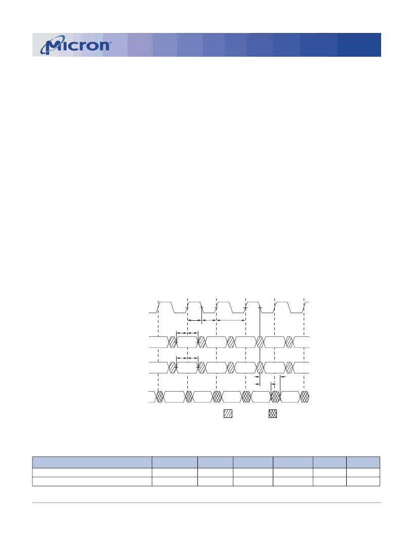
Figure 40: TAP Timing
Table 12:
+0°C = TC = +95°C; +1.7V = V
DD
= +1.9V, unless otherwise noted
TAP AC Electrical Characteristics and Operating Conditions
DESCRIPTION
CONDITIONS
SYMBOL
V
IH
V
IL
MIN
MAX
UNITS
V
V
NOTES
1, 2
1, 2
Input HIGH (Logic 1) Voltage
Input LOW (Logic 0) Voltage
V
REF
+ 0.3
V
SS
Q - 0.3
V
DD
+ 0.3
V
REF
- 0.3
tTLTH
Test Clock
(TCK)
1
2
3
4
5
6
Test Mode Select
(TMS)
tTHTL
Test Data-Out
(TDO)
tTHTH
Test Data-In
(TDI)
tTHMX
tMVTH
tTHDX
tDVTH
tTLOX
tTLOV
DON’T CARE
UNDEFINED
相關(guān)PDF資料 |
PDF描述 |
|---|---|
| MT49H32M9CFM-xx | 288Mb SIO REDUCED LATENCY(RLDRAM II) |
| MT4C1004J | 4 Meg x 1 FPM DRAM(4 M x 1快速頁面模式動態(tài)RAM) |
| MT4C4001STG-6 | standard or self refresh |
| MT4C4001STG-7 | standard or self refresh |
| MT4C4001STG-8 | standard or self refresh |
相關(guān)代理商/技術(shù)參數(shù) |
參數(shù)描述 |
|---|---|
| MT49H32M9CFM-25 | 制造商:Micron Technology Inc 功能描述:DRAM CHIP RLDRAM 288MBIT 1.8V 144FBGA - Trays |
| MT49H32M9CFM-33 | 制造商:Micron Technology Inc 功能描述:DRAM CHIP RLDRAM 288MBIT 1.8V 144FBGA - Trays |
| MT49H32M9CFM-5 | 制造商:Micron Technology Inc 功能描述:DRAM CHIP RLDRAM 288MBIT 1.8V 144FBGA - Tape and Reel |
| MT49H32M9CFM-XX | 制造商:MICRON 制造商全稱:Micron Technology 功能描述:288Mb SIO REDUCED LATENCY(RLDRAM II) |
| MT49H32M9CHU-25 | 制造商:Micron Technology Inc 功能描述:DRAM CHIP RLDRAM 288MBIT 1.8V 144FBGA - Trays |
發(fā)布緊急采購,3分鐘左右您將得到回復(fù)。