- 您現(xiàn)在的位置:買賣IC網(wǎng) > PDF目錄231503 > WEDPNF8M721V-1012BC SPECIALTY MEMORY CIRCUIT, PBGA275 PDF資料下載
參數(shù)資料
| 型號(hào): | WEDPNF8M721V-1012BC |
| 元件分類: | 存儲(chǔ)器 |
| 英文描述: | SPECIALTY MEMORY CIRCUIT, PBGA275 |
| 封裝: | 32 X 25 MM, PLASTIC, BGA-275 |
| 文件頁數(shù): | 3/42頁 |
| 文件大小: | 686K |
| 代理商: | WEDPNF8M721V-1012BC |
第1頁第2頁當(dāng)前第3頁第4頁第5頁第6頁第7頁第8頁第9頁第10頁第11頁第12頁第13頁第14頁第15頁第16頁第17頁第18頁第19頁第20頁第21頁第22頁第23頁第24頁第25頁第26頁第27頁第28頁第29頁第30頁第31頁第32頁第33頁第34頁第35頁第36頁第37頁第38頁第39頁第40頁第41頁第42頁
11
White Electronic Designs Corporation (602) 437-1520 www.whiteedc.com
WEDPNF8M721V-XBX
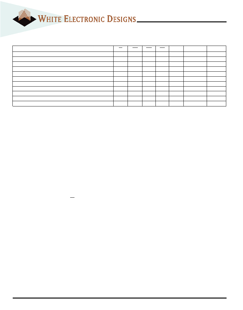
TABLE 3 TRUTH TABLE - COMMANDS AND DQM OPERATION (Note 1)
NAME (FUNCTION)
CS
RAS
CAS
WE
DQM
ADDR
I/Os
COMMAND INHIBIT (NOP)
H
X
NO OPERATION (NOP)
L
H
X
ACTIVE (Select bank and activate row) ( 3)
L
H
X
Bank/Row
X
READ (Select bank and column, and start READ burst) (4)
L
H
L
H
L/H 8
Bank/Col
X
WRITE (Select bank and column, and start WRITE burst) (4)
L
H
L
L/H 8
Bank/Col
Valid
BURST TERMINATE
L
H
L
X
Active
PRECHARGE (Deactivate row in bank or banks) ( 5)
L
H
L
X
Code
X
AUTO REFRESH or SELF REFRESH (Enter self refresh mode) (6, 7)
L
H
X
LOAD MODE REGISTER (2)
L
X
Op-Code
X
Write Enable/Output Enable (8)
–
L
–
Active
Write Inhibit/Output High-Z (8)
–
H
–
High-Z
NOTES:
1. CKE is HIGH for all commands shown except SELF REFRESH.
2. A0-11 define the op-code written to the Mode Register.
3. A0-11 provide row address, and BA0, BA1 determine which bank is made active.
4. A0-8 provide column address; A10 HIGH enables the auto precharge feature (nonpersistent), while A10 LOW disables the auto precharge feature; BA0, BA1
determine which bank is being read from or written to.
5. A10 LOW: BA0, BA1 determine the bank being precharged. A10 HIGH: All banks precharged and BA0, BA1 are “Don’t Care.”
6. This command is AUTO REFRESH if CKE is HIGH; SELF REFRESH if CKE is LOW.
7. Internal refresh counter controls row addressing; all inputs and I/Os are “Don’t Care” except for CKE.
8. Activates or deactivates the I/Os during WRITEs (zero-clock delay) and READs (two-clock delay).
READ
The READ command is used to initiate a burst read access to an
active row. The value on the BA0, BA1 inputs selects the bank, and
the address provided on inputs A0-8 selects the starting column
location. The value on input A10 determines whether or not AUTO
PRECHARGE is used. If AUTO PRECHARGE is selected, the row
being accessed will be precharged at the end of the READ burst;
if AUTO PRECHARGE is not selected, the row will remain open for
subsequent accesses. Read data appears on the I/Os subject to the
logic level on the DQM inputs two clocks earlier. If a given DQM signal
was registered HIGH, the corresponding I/Os will be High-Z two
clocks later; if the DQM signal was registered LOW, the I/Os will
provide valid data.
WRITE
The WRITE command is used to initiate a burst write access to an
active row. The value on the BA0, BA1 inputs selects the bank, and
the address provided on inputs A0-8 selects the starting column
location. The value on input A10 determines whether or not AUTO
PRECHARGE is used. If AUTO PRECHARGE is selected, the row being
accessed will be precharged at the end of the WRITE burst; if AUTO
PRECHARGE is not selected, the row will remain open for subsequent
accesses. Input data appearing on the I/Os is written to the memory
array subject to the DQM input logic level appearing coincident with
the data. If a given DQM signal is registered LOW, the corresponding
data will be written to memory; if the DQM signal is registered HIGH,
the corresponding data inputs will be ignored, and a WRITE will not
be executed to that byte/column location.
COMMAND INHIBIT
The COMMAND INHIBIT function prevents new commands from
being executed by the SDRAM, regardless of whether the CLK
signal is enabled. The SDRAM is effectively deselected. Opera-
tions already in progress are not affected.
NO OPERATION (NOP)
The NO OPERATION (NOP) command is used to perform a NOP to
an SDRAM which is selected (CS is LOW). This prevents unwanted
commands from being registered during idle or wait states. Op-
erations already in progress are not affected.
LOAD MODE REGISTER
The Mode Register is loaded via inputs A0-11. See Mode Register
heading in the Register Definition section. The LOAD MODE
REGISTER command can only be issued when all banks are idle,
and a subsequent executable command cannot be issued until
tMRD is met.
ACTIVE
The ACTIVE command is used to open (or activate) a row in a
particular bank for a subsequent access. The value on the BA0,
BA1 inputs selects the bank, and the address provided on inputs
A0-11 selects the row. This row remains active (or open) for
accesses until a PRECHARGE command is issued to that bank. A
PRECHARGE command must be issued before opening a different
row in the same bank.
相關(guān)PDF資料 |
PDF描述 |
|---|---|
| WE128K32-140G1UIA | 128K X 32 EEPROM 5V MODULE, 140 ns, CQFP68 |
| WE128K32-150G1UM | 128K X 32 EEPROM 5V MODULE, 150 ns, CQFP68 |
| WE128K32-200G1UMA | 128K X 32 EEPROM 5V MODULE, 200 ns, CQFP68 |
| WS128K32N-85HME | 512K X 8 MULTI DEVICE SRAM MODULE, 85 ns, CPGA66 |
| WSF512K16-72H2I | SPECIALTY MEMORY CIRCUIT, CPGA66 |
相關(guān)代理商/技術(shù)參數(shù) |
參數(shù)描述 |
|---|---|
| WEDPNF8M721V-1012BI | 制造商:未知廠家 制造商全稱:未知廠家 功能描述:8Mx72 Synchronous DRAM + 8Mb Flash Mixed Module Multi-Chip Package |
| WEDPNF8M721V-1012BM | 制造商:未知廠家 制造商全稱:未知廠家 功能描述:8Mx72 Synchronous DRAM + 8Mb Flash Mixed Module Multi-Chip Package |
| WEDPNF8M721V-1015BC | 制造商:未知廠家 制造商全稱:未知廠家 功能描述:8Mx72 Synchronous DRAM + 8Mb Flash Mixed Module Multi-Chip Package |
| WEDPNF8M721V-1015BI | 制造商:未知廠家 制造商全稱:未知廠家 功能描述:8Mx72 Synchronous DRAM + 8Mb Flash Mixed Module Multi-Chip Package |
| WEDPNF8M721V-1015BM | 制造商:未知廠家 制造商全稱:未知廠家 功能描述:8Mx72 Synchronous DRAM + 8Mb Flash Mixed Module Multi-Chip Package |
發(fā)布緊急采購,3分鐘左右您將得到回復(fù)。