- 您現(xiàn)在的位置:買賣IC網(wǎng) > PDF目錄383961 > TMX320DM6437BZDUA (Texas Instruments, Inc.) Digital Media Processor PDF資料下載
參數(shù)資料
| 型號: | TMX320DM6437BZDUA |
| 廠商: | Texas Instruments, Inc. |
| 英文描述: | Digital Media Processor |
| 中文描述: | 數(shù)字媒體處理器 |
| 文件頁數(shù): | 163/309頁 |
| 文件大?。?/td> | 2216K |
| 代理商: | TMX320DM6437BZDUA |
第1頁第2頁第3頁第4頁第5頁第6頁第7頁第8頁第9頁第10頁第11頁第12頁第13頁第14頁第15頁第16頁第17頁第18頁第19頁第20頁第21頁第22頁第23頁第24頁第25頁第26頁第27頁第28頁第29頁第30頁第31頁第32頁第33頁第34頁第35頁第36頁第37頁第38頁第39頁第40頁第41頁第42頁第43頁第44頁第45頁第46頁第47頁第48頁第49頁第50頁第51頁第52頁第53頁第54頁第55頁第56頁第57頁第58頁第59頁第60頁第61頁第62頁第63頁第64頁第65頁第66頁第67頁第68頁第69頁第70頁第71頁第72頁第73頁第74頁第75頁第76頁第77頁第78頁第79頁第80頁第81頁第82頁第83頁第84頁第85頁第86頁第87頁第88頁第89頁第90頁第91頁第92頁第93頁第94頁第95頁第96頁第97頁第98頁第99頁第100頁第101頁第102頁第103頁第104頁第105頁第106頁第107頁第108頁第109頁第110頁第111頁第112頁第113頁第114頁第115頁第116頁第117頁第118頁第119頁第120頁第121頁第122頁第123頁第124頁第125頁第126頁第127頁第128頁第129頁第130頁第131頁第132頁第133頁第134頁第135頁第136頁第137頁第138頁第139頁第140頁第141頁第142頁第143頁第144頁第145頁第146頁第147頁第148頁第149頁第150頁第151頁第152頁第153頁第154頁第155頁第156頁第157頁第158頁第159頁第160頁第161頁第162頁當前第163頁第164頁第165頁第166頁第167頁第168頁第169頁第170頁第171頁第172頁第173頁第174頁第175頁第176頁第177頁第178頁第179頁第180頁第181頁第182頁第183頁第184頁第185頁第186頁第187頁第188頁第189頁第190頁第191頁第192頁第193頁第194頁第195頁第196頁第197頁第198頁第199頁第200頁第201頁第202頁第203頁第204頁第205頁第206頁第207頁第208頁第209頁第210頁第211頁第212頁第213頁第214頁第215頁第216頁第217頁第218頁第219頁第220頁第221頁第222頁第223頁第224頁第225頁第226頁第227頁第228頁第229頁第230頁第231頁第232頁第233頁第234頁第235頁第236頁第237頁第238頁第239頁第240頁第241頁第242頁第243頁第244頁第245頁第246頁第247頁第248頁第249頁第250頁第251頁第252頁第253頁第254頁第255頁第256頁第257頁第258頁第259頁第260頁第261頁第262頁第263頁第264頁第265頁第266頁第267頁第268頁第269頁第270頁第271頁第272頁第273頁第274頁第275頁第276頁第277頁第278頁第279頁第280頁第281頁第282頁第283頁第284頁第285頁第286頁第287頁第288頁第289頁第290頁第291頁第292頁第293頁第294頁第295頁第296頁第297頁第298頁第299頁第300頁第301頁第302頁第303頁第304頁第305頁第306頁第307頁第308頁第309頁
www.ti.com
P
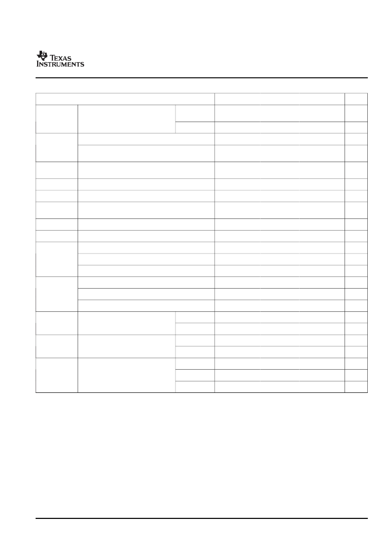
5.2 Recommended Operating Conditions
(1)
TMS320DM6437
Digital Media Processor
SPRS345B–NOVEMBER 2006–REVISED MARCH 2007
MIN
NOM
MAX
UNIT
(-600, -500, -400
devices)
1.14
1.2
1.26
V
CV
DD
Supply voltage, Core (CV
DD
, V
DDA_1P1V
)
(2)
(-400 devices)
1.0
1.05
1.1
V
Supply voltage, I/O, 3.3V (DV
DD33
)
3.14
3.3
3.46
V
DV
DD
Supply voltage, I/O, 1.8V (DV
DDR2
, DDR_VDDDLL, PLL
PWR18
,
V
DDA_1P8V
, MXV
DD(3)
)
1.71
1.8
1.89
V
Supply ground (V
SS
, V
SSA_1P8V
, V
SSA_1P1V
, DDR_VSSDLL,
MXV
SS(4)
)
V
SS
0
0
0
V
DDR_VREF
DDR2 reference voltage
(5)
0.49DV
DDR2
0.5DV
DDR2
0.51DV
DDR2
V
DDR_ZP
DDR2 impedance control, connected via 200
resistor to V
SS
V
SS
V
DDR2 impedance control, connected via 200
resistor to
DV
DDR2
DDR_ZN
DV
DDR2
V
DAC_VREF
DAC reference voltage input
0.475
0.5
0.525
V
DAC_RBIAS
DAC biasing, connected via 4 k
resistor to V
SSA_1P8V
V
SSA_1P8V
V
High-level input voltage, 3.3V (except PCI-capable and I2C pins)
2
V
V
IH
High-level input voltage, PCI
0.5DV
DD33
DV
DD33
+ 0.5
V
High-level input voltage, I2C
0.7DV
DD33
Low-level input voltage, 3.3V (except PCI-capable and I2C pins)
0.8
V
V
IL
Low-level input voltage, PCI
–0.5
0.3DV
DD33
V
Low-level input voltage, I2C
0
0.3DV
DD33
V
Commercial
0
90
°
C
T
J
Operating Junction temperature
(6)(7)
Extended
–40
125
°
C
Commercial
0
70
°
C
T
A
Operating Ambient temperature
(7)
Extended
-40
85
°
C
(-600 devices)
600
MHz
F
SYSCLK1
DSP Operating Frequency (SYSCLK1)
(-500 devices)
500
MHz
(-400 devices)
400
MHz
(1)
For -400 speed devices, either a 1.05-V
or
a 1.2-V core supply voltage can be used. The actual voltage
must
be determined at device
power-up, and
not
be changed dynamically during run-time.
Future variants of TI SoC devices may operate at voltages ranging from 0.9 V to 1.4 V to provide a range of system power/performance
options. TI highly recommends that users design-in a supply that can handle multiple voltages within this range (i.e., 1.0 V, 1.05 V,
1.1 V, 1.14 V, 1.2 V, 1.26 V with
±
3% tolerances) by implementing simple board changes such as reference resistor values or input pin
configuration modifications. Not incorporating a flexible supply may limit the system's ability to easily adapt to future versions of TI SoC
devices.
Oscillator 1.8 V power supply (MXV
) can be connected to the same 1.8 V power supply as DV
.
Oscillator ground (MXV
) must be kept separate from other grounds and connected directly to the crystal load capacitor ground.
DDR_VREF is expected to equal 0.5DV
of the transmitting device and to track variations in the DV
.
In the absence of a heat sink or direct thermal attachment on the top of the device, use the following formula to determine the device
junction temperature: T
= T
+ (Power x Psi
). Power and T
can be measured by the user.
Section 7.1
,
Thermal Data for ZWT
and
Section 7.1.1
,
Thermal Data for ZDU
provide the junction-to-package top (PSI
) value based on airflow in the system. In the presence
of a heat sink or direct thermal attachment on the top of the device, additional calculations and considerations
must
be taken into
account. For more detailed information on thermal considerations, measurements, and calculations, see the
TMS320DM643x Thermal
Considerations
Application Report (literuature number SPRAA
TBD
).
Applications must meet
both
the Operating Junction Temperature and Operating Ambient Temperature requirements. For more detailed
information on thermal considerations, measurements, and calculations, see the
TMS320DM643x Thermal Considerations
Application
Report (literuature number SPRAA
TBD).
(2)
(3)
(4)
(5)
(6)
(7)
Submit Documentation Feedback
Device Operating Conditions
163
相關PDF資料 |
PDF描述 |
|---|---|
| TMX320DM6437BZWTA | Digital Media Processor |
| TMS320DM6443_07 | Digital Media System-on-Chip |
| TMX320DM6443AZWT | Digital Media System-on-Chip |
| TMX320DM6443ZWT | Digital Media System-on-Chip |
| TMS320DM647_08 | Digital Media Processor |
相關代理商/技術參數(shù) |
參數(shù)描述 |
|---|---|
| TMX320DM6437BZWTA | 功能描述:數(shù)字信號處理器和控制器 - DSP, DSC Dig Media Processor RoHS:否 制造商:Microchip Technology 核心:dsPIC 數(shù)據(jù)總線寬度:16 bit 程序存儲器大小:16 KB 數(shù)據(jù) RAM 大小:2 KB 最大時鐘頻率:40 MHz 可編程輸入/輸出端數(shù)量:35 定時器數(shù)量:3 設備每秒兆指令數(shù):50 MIPs 工作電源電壓:3.3 V 最大工作溫度:+ 85 C 封裝 / 箱體:TQFP-44 安裝風格:SMD/SMT |
| TMX320DM6441CZWT | 制造商:Texas Instruments 功能描述: |
| TMX320DM6441DZWT | 制造商:Texas Instruments 功能描述:DAVINCI DIGITAL MEDIA SYSTEM-ON-CHIP - Tape and Reel |
| TMX320DM6443AZWT | 制造商:Rochester Electronics LLC 功能描述:DAVINCI DIGITAL MEDIA SYSTEM-ON-CHIP - Tape and Reel |
| TMX320DM6443BZWT | 制造商:Texas Instruments 功能描述: |
發(fā)布緊急采購,3分鐘左右您將得到回復。