- 您現(xiàn)在的位置:買賣IC網(wǎng) > PDF目錄385940 > TMS320C6713BGDPA200 (Texas Instruments, Inc.) FLOATING-POINT DIGITAL SIGNAL PROCESSORS PDF資料下載
參數(shù)資料
| 型號: | TMS320C6713BGDPA200 |
| 廠商: | Texas Instruments, Inc. |
| 元件分類: | 數(shù)字信號處理 |
| 英文描述: | FLOATING-POINT DIGITAL SIGNAL PROCESSORS |
| 中文描述: | 浮點數(shù)字信號處理器 |
| 文件頁數(shù): | 91/150頁 |
| 文件大?。?/td> | 2039K |
| 代理商: | TMS320C6713BGDPA200 |
第1頁第2頁第3頁第4頁第5頁第6頁第7頁第8頁第9頁第10頁第11頁第12頁第13頁第14頁第15頁第16頁第17頁第18頁第19頁第20頁第21頁第22頁第23頁第24頁第25頁第26頁第27頁第28頁第29頁第30頁第31頁第32頁第33頁第34頁第35頁第36頁第37頁第38頁第39頁第40頁第41頁第42頁第43頁第44頁第45頁第46頁第47頁第48頁第49頁第50頁第51頁第52頁第53頁第54頁第55頁第56頁第57頁第58頁第59頁第60頁第61頁第62頁第63頁第64頁第65頁第66頁第67頁第68頁第69頁第70頁第71頁第72頁第73頁第74頁第75頁第76頁第77頁第78頁第79頁第80頁第81頁第82頁第83頁第84頁第85頁第86頁第87頁第88頁第89頁第90頁當前第91頁第92頁第93頁第94頁第95頁第96頁第97頁第98頁第99頁第100頁第101頁第102頁第103頁第104頁第105頁第106頁第107頁第108頁第109頁第110頁第111頁第112頁第113頁第114頁第115頁第116頁第117頁第118頁第119頁第120頁第121頁第122頁第123頁第124頁第125頁第126頁第127頁第128頁第129頁第130頁第131頁第132頁第133頁第134頁第135頁第136頁第137頁第138頁第139頁第140頁第141頁第142頁第143頁第144頁第145頁第146頁第147頁第148頁第149頁第150頁
TMS320C6713, TMS320C6713B
FLOATING-POINT DIGITAL SIGNAL PROCESSORS
SPRS186I
DECEMBER 2001
REVISED MAY 2004
91
POST OFFICE BOX 1443
HOUSTON, TEXAS 77251
1443
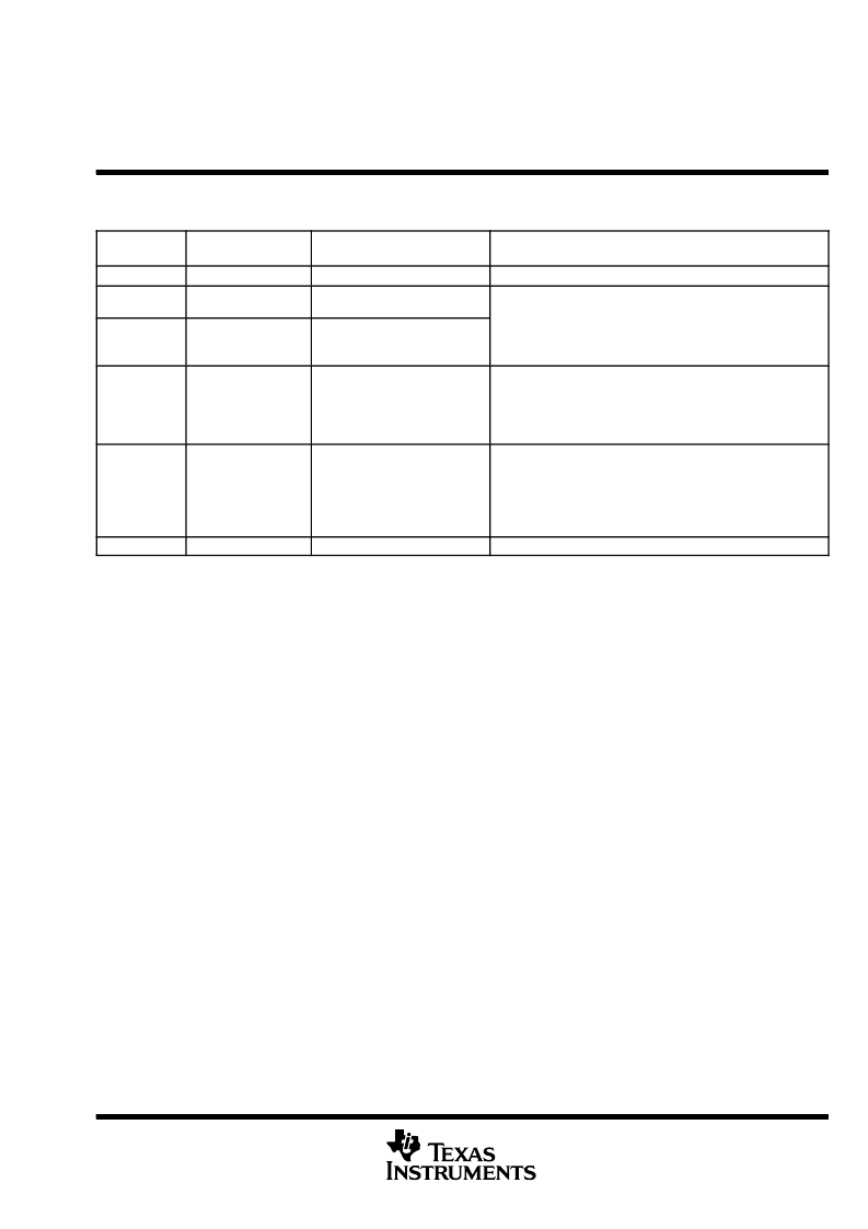
Table 45. Characteristics of the Power-Down Modes
PRWD FIELD
(BITS 15
10)
POWER-DOWN
MODE
WAKE-UP METHOD
EFFECT ON CHIP’S OPERATION
000000
No power-down
—
—
001001
PD1
Wake by an enabled interrupt
CPU halted (except for the interrupt logic)
Power-down mode blocks the internal clock inputs at the
Power down mode blocks the internal clock inputs at the
boundary of the CPU, preventing most of the CPU’s logic from
switching. During PD1, EDMA transactions can proceed
between peripherals and internal memory.
010001
PD1
Wake by an enabled or
non-enabled interrupt
011010
PD2
Wake by a device reset
Output clock from PLL is halted, stopping the internal clock
structure from switching and resulting in the entire chip being
halted. All register and internal RAM contents are preserved. All
functional I/O “freeze” in the last state when the PLL clock is
turned off.
011100
PD3
Wake by a device reset
Input clock to the PLL stops generating clocks. All register and
internal RAM contents are preserved. All functional I/O “freeze” in
the last state when the PLL clock is turned off. Following reset, the
PLL needs time to re-lock, just as it does following power-up.
Wake-up from PD3 takes longer than wake-up from PD2 because
the PLL needs to be re-locked, just as it does following power-up.
—
All others
When entering PD2 and PD3, all functional I/O remains in the previous state. However, for peripherals which are asynchronous in nature or
peripherals with an external clock source, output signals may transition in response to stimulus on the inputs. Under these conditions,
peripherals will not operate according to specifications.
Reserved
—
On C6713B silicon revision 2.0 and C6713 silicon revision 1.1, the device includes a programmable PLL which
allows software control of PLL bypass via the PLLEN bit in the PLLCSR register. With this enhanced functionality
comes some additional considerations when entering power-down modes.
The power-down modes (PD2 and PD3) function by disabling the PLL to stop clocks to the device. However,
if the PLL is bypassed (PLLEN = 0), the device will still receive clocks from the external clock input (CLKIN).
Therefore, bypassing the PLL makes the power-down modes PD2 and PD3 ineffective.
Make sure that the PLL is enabled by writing a “1” to PLLEN bit (PLLCSR.0) before writing to either PD3
(CSR.11) or PD2 (CSR.10) to enter a power-down mode.
power-supply sequencing
TI DSPs do not require specific power sequencing between the core supply and the I/O supply. However,
systems should be designed to ensure that neither supply is powered up for extended periods of time
(
>
1 second) if the other supply is below the proper operating voltage.
system-level design considerations
System-level design considerations, such as bus contention, may require supply sequencing to be
implemented. In this case, the core supply should be powered up prior to (and powered down after), the I/O
buffers. This is to ensure that the I/O buffers receive valid inputs from the core before the output buffers are
powered up, thus, preventing bus contention with other chips on the board.
相關(guān)PDF資料 |
PDF描述 |
|---|---|
| TMS320C6727BGDH275 | Floating-Point Digital Signal Processors |
| TMS320F28044GGMA | Digital Signal Processor |
| TMS320F28044GGMQ | Digital Signal Processor |
| TMS320F28044GGMS | Digital Signal Processor |
| TMS320F28044PZQ | Digital Signal Processor |
相關(guān)代理商/技術(shù)參數(shù) |
參數(shù)描述 |
|---|---|
| TMS320C6713BGDP-C20 | 制造商:Texas Instruments 功能描述: |
| TMS320C6713BPYP167 | 制造商:TI 功能描述:_ |
| TMS320C6713BPYP200 | 功能描述:數(shù)字信號處理器和控制器 - DSP, DSC Floating-Pt Dig Sig Processors RoHS:否 制造商:Microchip Technology 核心:dsPIC 數(shù)據(jù)總線寬度:16 bit 程序存儲器大小:16 KB 數(shù)據(jù) RAM 大小:2 KB 最大時鐘頻率:40 MHz 可編程輸入/輸出端數(shù)量:35 定時器數(shù)量:3 設(shè)備每秒兆指令數(shù):50 MIPs 工作電源電壓:3.3 V 最大工作溫度:+ 85 C 封裝 / 箱體:TQFP-44 安裝風格:SMD/SMT |
| TMS320C6713BPYP225 | 制造商:Texas Instruments 功能描述: |
| TMS320C6713BZDP225 | 功能描述:數(shù)字信號處理器和控制器 - DSP, DSC Floating-Pt Dig Sig Processors RoHS:否 制造商:Microchip Technology 核心:dsPIC 數(shù)據(jù)總線寬度:16 bit 程序存儲器大小:16 KB 數(shù)據(jù) RAM 大小:2 KB 最大時鐘頻率:40 MHz 可編程輸入/輸出端數(shù)量:35 定時器數(shù)量:3 設(shè)備每秒兆指令數(shù):50 MIPs 工作電源電壓:3.3 V 最大工作溫度:+ 85 C 封裝 / 箱體:TQFP-44 安裝風格:SMD/SMT |
發(fā)布緊急采購,3分鐘左右您將得到回復(fù)。