- 您現(xiàn)在的位置:買賣IC網(wǎng) > PDF目錄385940 > TMS320C6713BGDPA200 (Texas Instruments, Inc.) FLOATING-POINT DIGITAL SIGNAL PROCESSORS PDF資料下載
參數(shù)資料
| 型號(hào): | TMS320C6713BGDPA200 |
| 廠商: | Texas Instruments, Inc. |
| 元件分類: | 數(shù)字信號(hào)處理 |
| 英文描述: | FLOATING-POINT DIGITAL SIGNAL PROCESSORS |
| 中文描述: | 浮點(diǎn)數(shù)字信號(hào)處理器 |
| 文件頁數(shù): | 120/150頁 |
| 文件大小: | 2039K |
| 代理商: | TMS320C6713BGDPA200 |
第1頁第2頁第3頁第4頁第5頁第6頁第7頁第8頁第9頁第10頁第11頁第12頁第13頁第14頁第15頁第16頁第17頁第18頁第19頁第20頁第21頁第22頁第23頁第24頁第25頁第26頁第27頁第28頁第29頁第30頁第31頁第32頁第33頁第34頁第35頁第36頁第37頁第38頁第39頁第40頁第41頁第42頁第43頁第44頁第45頁第46頁第47頁第48頁第49頁第50頁第51頁第52頁第53頁第54頁第55頁第56頁第57頁第58頁第59頁第60頁第61頁第62頁第63頁第64頁第65頁第66頁第67頁第68頁第69頁第70頁第71頁第72頁第73頁第74頁第75頁第76頁第77頁第78頁第79頁第80頁第81頁第82頁第83頁第84頁第85頁第86頁第87頁第88頁第89頁第90頁第91頁第92頁第93頁第94頁第95頁第96頁第97頁第98頁第99頁第100頁第101頁第102頁第103頁第104頁第105頁第106頁第107頁第108頁第109頁第110頁第111頁第112頁第113頁第114頁第115頁第116頁第117頁第118頁第119頁當(dāng)前第120頁第121頁第122頁第123頁第124頁第125頁第126頁第127頁第128頁第129頁第130頁第131頁第132頁第133頁第134頁第135頁第136頁第137頁第138頁第139頁第140頁第141頁第142頁第143頁第144頁第145頁第146頁第147頁第148頁第149頁第150頁
TMS320C6713, TMS320C6713B
FLOATING-POINT DIGITAL SIGNAL PROCESSORS
SPRS186I
DECEMBER 2001
REVISED MAY 2004
120
POST OFFICE BOX 1443
HOUSTON, TEXAS 77251
1443
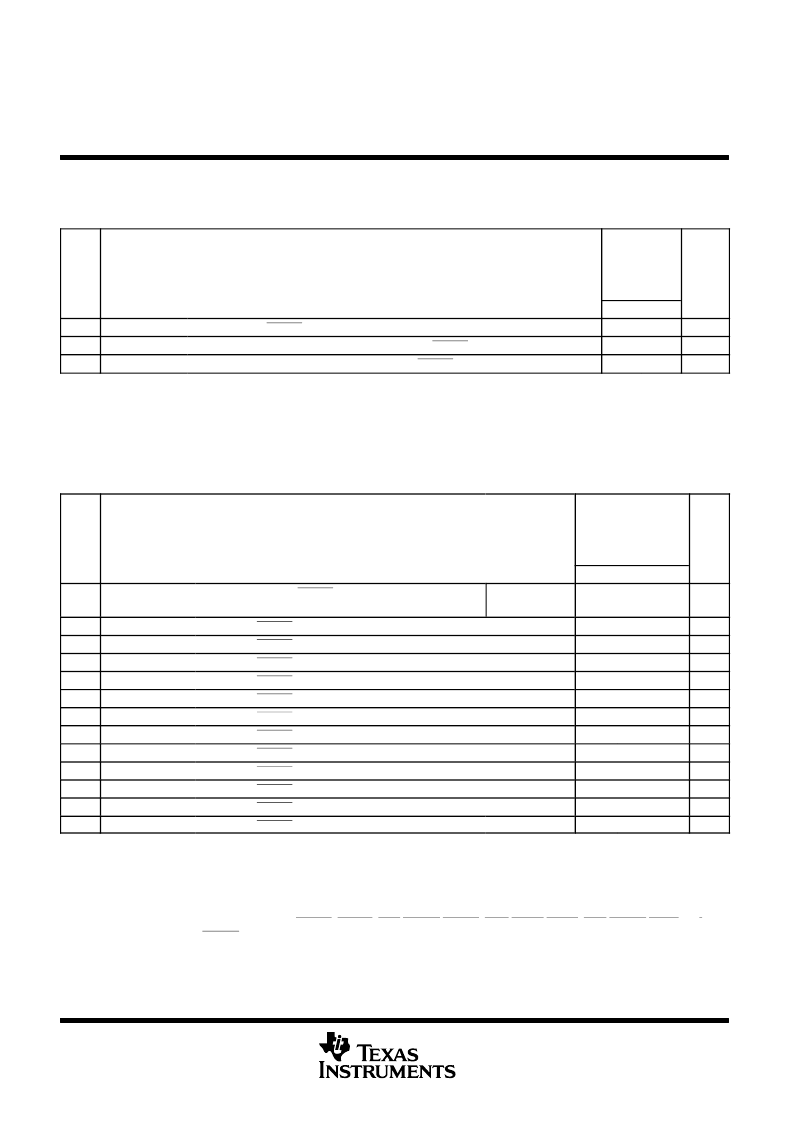
RESET TIMING
timing requirements for reset
(see Figure 47)
NO.
PYPA
167
PYP
200
GDPA
200
GDP
225
GDP
300
UNIT
MIN
100
2P
2P
MAX
1
13
14
t
w(RST)
t
su(HD)
t
h(HD)
Pulse duration, RESET
Setup time, HD boot configuration bits valid before RESET high
§
Hold time, HD boot configuration bits valid after RESET high
§
P = 1/CPU clock frequency in ns. For example, when running parts at 300 MHz, use P = 3.3 ns.
For the C6713/13B device, the PLL is bypassed immediately after the device comes out of reset. The PLL Controller can be programmed to
change the PLL mode in software. For more detailed information on the PLL Controller, see the
TMS320C6000 DSP Phase-Lock Loop (PLL)
Controller Peripheral Reference Guide
(literature number SPRU233).
§
The Boot and device configurations bits are latched asynchronously when RESET is transitioning high. The Boot and device configurations bits
consist of: HD[14, 8, 4:3].
ns
ns
ns
switching characteristics over recommended operating conditions during reset
(see Figure 47)
NO.
PARAMETER
PYPA
167
PYP
200
GDPA
200
GDP
225
GDP
300
UNIT
MIN
MAX
2
t
d(RSTH-ZV)
Delay time, external RESET high to internal reset high and
all signal groups valid
#||
CLKMODE0 = 1
512 x CLKIN
period
ns
3a
3b
4
5a
5b
6
7
8
9
10
11
12
t
d(RSTL-ECKOL)
t
d(RSTL-ECKOL)
t
d(RSTH-ECKOV)
t
d(RSTL-CKO2IV)
t
d(RSTL-CKO2IV)
t
d(RSTH-CKO2V)
t
d(RSTL-CKO3L)
t
d(RSTH-CKO3V)
t
d(RSTL-EMIFZHZ)
t
d(RSTL-EMIFLIV)
t
d(RSTL-Z1HZ)
t
d(RSTL-Z2HZ)
Delay time, RESET low to ECLKOUT low (6713)
Delay time, RESET low to ECLKOUT high impedance (6713B)
Delay time, RESET high to ECLKOUT valid
Delay time, RESET low to CLKOUT2 invalid (6713)
Delay time, RESET low to CLKOUT2 high impedance (6713B)
Delay time, RESET high to CLKOUT2 valid
Delay time, RESET low to CLKOUT3 low
Delay time, RESET high to CLKOUT3 valid
Delay time, RESET low to EMIF Z group high impedance
||
Delay time, RESET low to EMIF low group (BUSREQ) invalid
||
Delay time, RESET low to Z group 1 high impedance
||
Delay time, RESET low to Z group 2 high impedance
||
P = 1/CPU clock frequency in ns.
Note that while internal reset is asserted low, the CPU clock (SYSCLK1) period is equal to the input clock (CLKIN) period multiplied by 8. For
example, if the CLKIN period is 20 ns, then the CPU clock (SYSCLK1) period is 20 ns x 8 = 160 ns. Therefore, P = SYSCLK1 = 160 ns while
internal reset is asserted.
#
The internal reset is stretched exactly 512 x CLKIN cycles if CLKIN is used (CLKMODE0 = 1). If the input clock (CLKIN) is not stable when RESET
is deasserted, the actual delay time may vary.
||
EMIF Z group consists of:
EA[21:2], ED[31:0], CE[3:0], BE[3:0], ARE/SDCAS/SSADS, AWE/SDWE/SSWE, AOE/SDRAS/SSOE and
HOLDA
EMIF low group consists of: BUSREQ
Z group 1 consists of:
CLKR0/ACLKR0, CLKR1/AXR0[6], CLKX0/ACLKX0, CLKX1/AMUTE0, FSR0/AFSR0, FSR1/AXR0[7],
FSX0/AFSX0, FSX1, DX0/AXR0[1], DX1/AXR0[5], TOUT0/AXR0[2], TOUT1/AXR0[4], SDA0 and SCL0.
Z group 2 consists of:
All other HPI, McASP0/1, GPIO, and I2C1 signals.
0
0
ns
ns
ns
ns
ns
ns
ns
ns
ns
ns
ns
ns
6P
0
0
6P
0
6P
0
0
0
0
相關(guān)PDF資料 |
PDF描述 |
|---|---|
| TMS320C6727BGDH275 | Floating-Point Digital Signal Processors |
| TMS320F28044GGMA | Digital Signal Processor |
| TMS320F28044GGMQ | Digital Signal Processor |
| TMS320F28044GGMS | Digital Signal Processor |
| TMS320F28044PZQ | Digital Signal Processor |
相關(guān)代理商/技術(shù)參數(shù) |
參數(shù)描述 |
|---|---|
| TMS320C6713BGDP-C20 | 制造商:Texas Instruments 功能描述: |
| TMS320C6713BPYP167 | 制造商:TI 功能描述:_ |
| TMS320C6713BPYP200 | 功能描述:數(shù)字信號(hào)處理器和控制器 - DSP, DSC Floating-Pt Dig Sig Processors RoHS:否 制造商:Microchip Technology 核心:dsPIC 數(shù)據(jù)總線寬度:16 bit 程序存儲(chǔ)器大小:16 KB 數(shù)據(jù) RAM 大小:2 KB 最大時(shí)鐘頻率:40 MHz 可編程輸入/輸出端數(shù)量:35 定時(shí)器數(shù)量:3 設(shè)備每秒兆指令數(shù):50 MIPs 工作電源電壓:3.3 V 最大工作溫度:+ 85 C 封裝 / 箱體:TQFP-44 安裝風(fēng)格:SMD/SMT |
| TMS320C6713BPYP225 | 制造商:Texas Instruments 功能描述: |
| TMS320C6713BZDP225 | 功能描述:數(shù)字信號(hào)處理器和控制器 - DSP, DSC Floating-Pt Dig Sig Processors RoHS:否 制造商:Microchip Technology 核心:dsPIC 數(shù)據(jù)總線寬度:16 bit 程序存儲(chǔ)器大小:16 KB 數(shù)據(jù) RAM 大小:2 KB 最大時(shí)鐘頻率:40 MHz 可編程輸入/輸出端數(shù)量:35 定時(shí)器數(shù)量:3 設(shè)備每秒兆指令數(shù):50 MIPs 工作電源電壓:3.3 V 最大工作溫度:+ 85 C 封裝 / 箱體:TQFP-44 安裝風(fēng)格:SMD/SMT |
發(fā)布緊急采購,3分鐘左右您將得到回復(fù)。