- 您現(xiàn)在的位置:買賣IC網(wǎng) > PDF目錄383876 > T7256A Compliance with the New ETSI PSD Requirement PDF資料下載
參數(shù)資料
| 型號: | T7256A |
| 英文描述: | Compliance with the New ETSI PSD Requirement |
| 中文描述: | 符合新的ETSI PSD的要求 |
| 文件頁數(shù): | 75/116頁 |
| 文件大?。?/td> | 1056K |
| 代理商: | T7256A |
第1頁第2頁第3頁第4頁第5頁第6頁第7頁第8頁第9頁第10頁第11頁第12頁第13頁第14頁第15頁第16頁第17頁第18頁第19頁第20頁第21頁第22頁第23頁第24頁第25頁第26頁第27頁第28頁第29頁第30頁第31頁第32頁第33頁第34頁第35頁第36頁第37頁第38頁第39頁第40頁第41頁第42頁第43頁第44頁第45頁第46頁第47頁第48頁第49頁第50頁第51頁第52頁第53頁第54頁第55頁第56頁第57頁第58頁第59頁第60頁第61頁第62頁第63頁第64頁第65頁第66頁第67頁第68頁第69頁第70頁第71頁第72頁第73頁第74頁當前第75頁第76頁第77頁第78頁第79頁第80頁第81頁第82頁第83頁第84頁第85頁第86頁第87頁第88頁第89頁第90頁第91頁第92頁第93頁第94頁第95頁第96頁第97頁第98頁第99頁第100頁第101頁第102頁第103頁第104頁第105頁第106頁第107頁第108頁第109頁第110頁第111頁第112頁第113頁第114頁第115頁第116頁
Data Sheet
January 1998
T7256 Single-Chip NT1 (SCNT1) Transceiver
Lucent Technologies Inc.
71
Application Briefs
(continued)
Available Tools for Evaluation of the T7256
(continued)
IMPORTANT NOTE:
In order to use the SPEC_V2 with your product, you must adhere to the following guidelines:
I
Make sure none of the signals in the Signal Name column of Table 34 are hardwired to V
CC
or GND (with the
exception of GND
D
). If you need to tie any of these signals high or low, do it through a 5.1 k
resistor.
I
Make sure that circuitry on your board that is driving any of the Signal Name signals can be disabled (3-stated,
open collector output driver turned off, or signal trace cut, if necessary) when using the SPEC_V2.
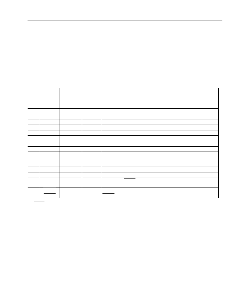
Table 34. SPEC_V2 Interface Connector Pinouts
*
If RESET is not connected, the T7237/56 will not be RESET when exiting mode 2 or 3. If this is the case, the UUT must be powered down to
get the SCNT1 out of test mode.
J1
Pin
#
Signal
Name
SPEC_V2
Input/
Output
X
—
X
—
O
I
I
I
O
I
—
T7237/
56 Pin #
Notes
1
2
3
4
5
6
7
8
9
10
11
GND
D
—
GND
D
—
SCK
CKOUT
INT
SDO
SDI
PS1E
—
16
—
10
—
15
17
11
14
12
9
—
—
Connects to V
DDD
when interfacing to SCNT1-RDB.
—
—
—
—
—
—
—
PS1E becomes an output from T7237/56 in test mode.
Connects to PS2E (T7237/56 pin #8) when interfacing to
SCNT1_RDB.
12
13
14
TDMDI
SYN8K
—
I
7
4
—
—
—
O
—
Connects to ILOSS (T7237/56 pin #6) when interfacing to SCNT1-
RDB.
Recommended but not mandatory.*
HIGHZ becomes an output from T7237/56 in test mode.
15
16
RESET
HIGHZ
O
I
43
44
相關PDF資料 |
PDF描述 |
|---|---|
| T7288 | CEPT/E1 Line Interface(CEPT/E1 線接口) |
| T7290A | DS1/T1/CEPT/E1 Line Interface(DS1/T1/CEPT/E1 線接口) |
| T7295-1 | E3 Integrated Line Receiver(E3 集成線接收器) |
| T7295-6 | DS3/SONET STS-1 Integrated Line Receiver(DS3/SONET STS-1 集成線接收器) |
| T7296 | Integrated Line Transmitter(集成PCM線傳送器) |
相關代理商/技術參數(shù) |
參數(shù)描述 |
|---|---|
| T7257 | 制造商:TE Connectivity 功能描述: |
| T-726 | 制造商:RHOMBUS-IND 制造商全稱:Rhombus Industries Inc. 功能描述:ADSL Line Interface Transformers |
| T7263 | 制造商:TE Connectivity 功能描述: |
| T7263A | 制造商:Toshiba America Electronic Components 功能描述:T7263A |
| T7264 | 制造商:TE Connectivity 功能描述: |
發(fā)布緊急采購,3分鐘左右您將得到回復。