- 您現(xiàn)在的位置:買(mǎi)賣(mài)IC網(wǎng) > PDF目錄383723 > OR3TP12-6PS240I Quad 2.3V 10 MHz OP, I temp, -40C to +85C, 14-SOIC 150mil, T/R PDF資料下載
參數(shù)資料
| 型號(hào): | OR3TP12-6PS240I |
| 英文描述: | Quad 2.3V 10 MHz OP, I temp, -40C to +85C, 14-SOIC 150mil, T/R |
| 中文描述: | 用戶(hù)可編程ASIC的特殊功能 |
| 文件頁(yè)數(shù): | 41/128頁(yè) |
| 文件大小: | 2450K |
| 代理商: | OR3TP12-6PS240I |
第1頁(yè)第2頁(yè)第3頁(yè)第4頁(yè)第5頁(yè)第6頁(yè)第7頁(yè)第8頁(yè)第9頁(yè)第10頁(yè)第11頁(yè)第12頁(yè)第13頁(yè)第14頁(yè)第15頁(yè)第16頁(yè)第17頁(yè)第18頁(yè)第19頁(yè)第20頁(yè)第21頁(yè)第22頁(yè)第23頁(yè)第24頁(yè)第25頁(yè)第26頁(yè)第27頁(yè)第28頁(yè)第29頁(yè)第30頁(yè)第31頁(yè)第32頁(yè)第33頁(yè)第34頁(yè)第35頁(yè)第36頁(yè)第37頁(yè)第38頁(yè)第39頁(yè)第40頁(yè)當(dāng)前第41頁(yè)第42頁(yè)第43頁(yè)第44頁(yè)第45頁(yè)第46頁(yè)第47頁(yè)第48頁(yè)第49頁(yè)第50頁(yè)第51頁(yè)第52頁(yè)第53頁(yè)第54頁(yè)第55頁(yè)第56頁(yè)第57頁(yè)第58頁(yè)第59頁(yè)第60頁(yè)第61頁(yè)第62頁(yè)第63頁(yè)第64頁(yè)第65頁(yè)第66頁(yè)第67頁(yè)第68頁(yè)第69頁(yè)第70頁(yè)第71頁(yè)第72頁(yè)第73頁(yè)第74頁(yè)第75頁(yè)第76頁(yè)第77頁(yè)第78頁(yè)第79頁(yè)第80頁(yè)第81頁(yè)第82頁(yè)第83頁(yè)第84頁(yè)第85頁(yè)第86頁(yè)第87頁(yè)第88頁(yè)第89頁(yè)第90頁(yè)第91頁(yè)第92頁(yè)第93頁(yè)第94頁(yè)第95頁(yè)第96頁(yè)第97頁(yè)第98頁(yè)第99頁(yè)第100頁(yè)第101頁(yè)第102頁(yè)第103頁(yè)第104頁(yè)第105頁(yè)第106頁(yè)第107頁(yè)第108頁(yè)第109頁(yè)第110頁(yè)第111頁(yè)第112頁(yè)第113頁(yè)第114頁(yè)第115頁(yè)第116頁(yè)第117頁(yè)第118頁(yè)第119頁(yè)第120頁(yè)第121頁(yè)第122頁(yè)第123頁(yè)第124頁(yè)第125頁(yè)第126頁(yè)第127頁(yè)第128頁(yè)
Lucent Technologies Inc.
Lucent Technologies Inc.
41
Data Sheet
March 2000
ORCA OR3TP12 FPSC
Embedded Master/Target PCI Interface
PCI Bus Core Master Controller Detailed Description
(continued)
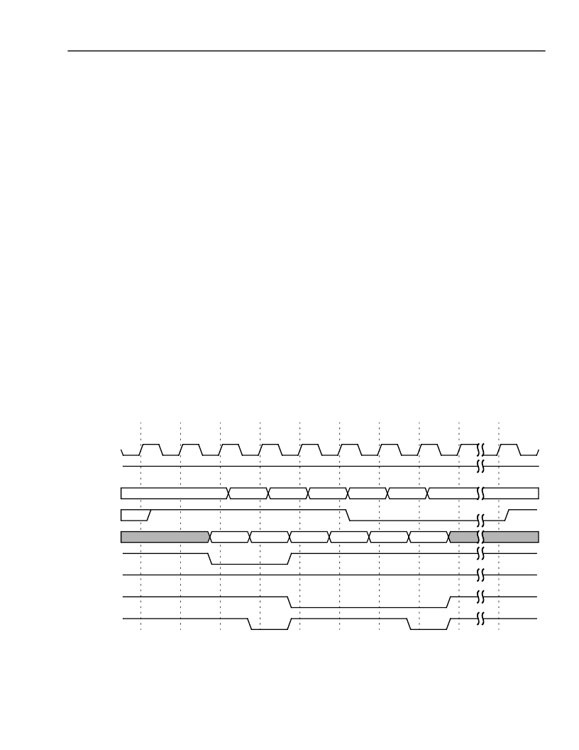
Example: Master Write, Burst Transaction
Figure 6 and Figure 7 show the timing of a Master write of four 32-bit data words, on the dual-port FPGA interface
and quad-port FPGA interface, respectively. In Figure 6, the command/address phase is initiated by the FPGA
application asserting Master address enable (
maenn
), while providing the Master command word on bus
datafmf-
pga
. On the next clock, the FPGA application provides the 32-bit address and ends the command/address phase
by asserting
mwlastcycn
.
To enter the data phase,
maenn
is deasserted,
mwdataenn
is asserted, and a valid 32-bit Dword of data provided
on bus
datafmfpga
. After the second write data word is provided,
ma_fulln
goes active indicating the Master will
be begin negotiating for the PCI bus (assuming
mwpcihold
is deaserted). The FPGA application continues to sup-
ply data (three 32-bit Dwords) on bus
datafmfpga
with
mwdataenn
asserted, while monitoring the
mw_fulln
flag.
To indicate the completion of the data phase,
mwlastcycn
is asserted, along with
mwdataenn
, during the final
data word.
For quad-port mode (Figure 7), the command/address and write data is transferred on the bus
mwdata
. The 18-bit
Master command will remain unchanged, but the 32-bit address will be split into two 16-bit components with the
LSB being transferred first. The command/address phase will require three clock cycles (with
maenn
asserted),
and
mwlastcycn
will be asserted on the final or MSB component of the address.
The quad-port data phase will also require additional clock cycles to transfer the four 32-bit write data word across
the bus
mwdata
. Similar to above, the data phase will be entered with the deassertion of
maenn
and assertion of
mwdataenn
.
mwlastcycn
will be deasserted for all write data words, except being asserted for the final 16-bit
MSB component.
Execution begins on the PCI bus, as shown in Figure 8, which shows the timing with an external Target. The trans-
action runs to normal completion. It is a typical PCI transaction (the remote Target supports fast decode), and the
protocol and timing are as required by the PCI Specification.
5-7351(F)
Figure 6. Master Write Burst (FIFO Interface, Dual-Port)
T0
T1
T2
T3
T4
T5
T6
T7
T8
0
1
A
B
A
B
0
CMD
ADRS
D0
D1
D2
D3
fclk
m_ready
mstatecntr
ma_fulln
datafmfpga
maenn
mw_fulln
mwdataenn
mwlastcycn
相關(guān)PDF資料 |
PDF描述 |
|---|---|
| OR3TP12 | Field-Programmable System Chip (FPSC) Embedded Master/Target PCI Interface |
| OR62 | OR62 is a 6-input OR gate with 2x drive strength |
| OR73 | 7-input OR gate with 3x drive strength. |
| OR8GU41 | DIFFUSED TYPE (HIGH SPEED RECTIFIER APPLICATIONS) |
| ORCAORT4622 | Field-Programmable System Chip (FPSC) Four-Channel x 622 Mbits/s Backplane Transceiver |
相關(guān)代理商/技術(shù)參數(shù) |
參數(shù)描述 |
|---|---|
| OR3TP127BA256-DB | 功能描述:FPGA - 現(xiàn)場(chǎng)可編程門(mén)陣列 2016 LUT 187 I/O RoHS:否 制造商:Altera Corporation 系列:Cyclone V E 柵極數(shù)量: 邏輯塊數(shù)量:943 內(nèi)嵌式塊RAM - EBR:1956 kbit 輸入/輸出端數(shù)量:128 最大工作頻率:800 MHz 工作電源電壓:1.1 V 最大工作溫度:+ 70 C 安裝風(fēng)格:SMD/SMT 封裝 / 箱體:FBGA-256 |
| OR3TP127BA352-DB | 功能描述:FPGA - 現(xiàn)場(chǎng)可編程門(mén)陣列 2016 LUT 187 I/O RoHS:否 制造商:Altera Corporation 系列:Cyclone V E 柵極數(shù)量: 邏輯塊數(shù)量:943 內(nèi)嵌式塊RAM - EBR:1956 kbit 輸入/輸出端數(shù)量:128 最大工作頻率:800 MHz 工作電源電壓:1.1 V 最大工作溫度:+ 70 C 安裝風(fēng)格:SMD/SMT 封裝 / 箱體:FBGA-256 |
| OR4 | 制造商:LATTICE 制造商全稱(chēng):Lattice Semiconductor 功能描述:ORCASeries 4 FPGAs |
| OR-401045290 | 制造商:ORTRONICS 功能描述:ORTRONICS 24 PORT MODULAR PATCH PANEL |
| OR40300011 | 制造商:ORTRONICS 功能描述:WORSTATION |
發(fā)布緊急采購(gòu),3分鐘左右您將得到回復(fù)。