- 您現(xiàn)在的位置:買賣IC網(wǎng) > PDF目錄383995 > TE3-MUX (INFINEON TECHNOLOGIES AG) Ultraframer DS3/E3/DS2/E2/DS1/E1/DS0 PDF資料下載
參數(shù)資料
| 型號(hào): | TE3-MUX |
| 廠商: | INFINEON TECHNOLOGIES AG |
| 元件分類: | 通信及網(wǎng)絡(luò) |
| 英文描述: | Ultraframer DS3/E3/DS2/E2/DS1/E1/DS0 |
| 中文描述: | Ultraframer DS3/E3/DS2/E2/DS1/E1/DS0 |
| 文件頁(yè)數(shù): | 70/211頁(yè) |
| 文件大?。?/td> | 2567K |
| 代理商: | TE3-MUX |
第1頁(yè)第2頁(yè)第3頁(yè)第4頁(yè)第5頁(yè)第6頁(yè)第7頁(yè)第8頁(yè)第9頁(yè)第10頁(yè)第11頁(yè)第12頁(yè)第13頁(yè)第14頁(yè)第15頁(yè)第16頁(yè)第17頁(yè)第18頁(yè)第19頁(yè)第20頁(yè)第21頁(yè)第22頁(yè)第23頁(yè)第24頁(yè)第25頁(yè)第26頁(yè)第27頁(yè)第28頁(yè)第29頁(yè)第30頁(yè)第31頁(yè)第32頁(yè)第33頁(yè)第34頁(yè)第35頁(yè)第36頁(yè)第37頁(yè)第38頁(yè)第39頁(yè)第40頁(yè)第41頁(yè)第42頁(yè)第43頁(yè)第44頁(yè)第45頁(yè)第46頁(yè)第47頁(yè)第48頁(yè)第49頁(yè)第50頁(yè)第51頁(yè)第52頁(yè)第53頁(yè)第54頁(yè)第55頁(yè)第56頁(yè)第57頁(yè)第58頁(yè)第59頁(yè)第60頁(yè)第61頁(yè)第62頁(yè)第63頁(yè)第64頁(yè)第65頁(yè)第66頁(yè)第67頁(yè)第68頁(yè)第69頁(yè)當(dāng)前第70頁(yè)第71頁(yè)第72頁(yè)第73頁(yè)第74頁(yè)第75頁(yè)第76頁(yè)第77頁(yè)第78頁(yè)第79頁(yè)第80頁(yè)第81頁(yè)第82頁(yè)第83頁(yè)第84頁(yè)第85頁(yè)第86頁(yè)第87頁(yè)第88頁(yè)第89頁(yè)第90頁(yè)第91頁(yè)第92頁(yè)第93頁(yè)第94頁(yè)第95頁(yè)第96頁(yè)第97頁(yè)第98頁(yè)第99頁(yè)第100頁(yè)第101頁(yè)第102頁(yè)第103頁(yè)第104頁(yè)第105頁(yè)第106頁(yè)第107頁(yè)第108頁(yè)第109頁(yè)第110頁(yè)第111頁(yè)第112頁(yè)第113頁(yè)第114頁(yè)第115頁(yè)第116頁(yè)第117頁(yè)第118頁(yè)第119頁(yè)第120頁(yè)第121頁(yè)第122頁(yè)第123頁(yè)第124頁(yè)第125頁(yè)第126頁(yè)第127頁(yè)第128頁(yè)第129頁(yè)第130頁(yè)第131頁(yè)第132頁(yè)第133頁(yè)第134頁(yè)第135頁(yè)第136頁(yè)第137頁(yè)第138頁(yè)第139頁(yè)第140頁(yè)第141頁(yè)第142頁(yè)第143頁(yè)第144頁(yè)第145頁(yè)第146頁(yè)第147頁(yè)第148頁(yè)第149頁(yè)第150頁(yè)第151頁(yè)第152頁(yè)第153頁(yè)第154頁(yè)第155頁(yè)第156頁(yè)第157頁(yè)第158頁(yè)第159頁(yè)第160頁(yè)第161頁(yè)第162頁(yè)第163頁(yè)第164頁(yè)第165頁(yè)第166頁(yè)第167頁(yè)第168頁(yè)第169頁(yè)第170頁(yè)第171頁(yè)第172頁(yè)第173頁(yè)第174頁(yè)第175頁(yè)第176頁(yè)第177頁(yè)第178頁(yè)第179頁(yè)第180頁(yè)第181頁(yè)第182頁(yè)第183頁(yè)第184頁(yè)第185頁(yè)第186頁(yè)第187頁(yè)第188頁(yè)第189頁(yè)第190頁(yè)第191頁(yè)第192頁(yè)第193頁(yè)第194頁(yè)第195頁(yè)第196頁(yè)第197頁(yè)第198頁(yè)第199頁(yè)第200頁(yè)第201頁(yè)第202頁(yè)第203頁(yè)第204頁(yè)第205頁(yè)第206頁(yè)第207頁(yè)第208頁(yè)第209頁(yè)第210頁(yè)第211頁(yè)
PEB 3445 E
Interface Description
Data Sheet
70
2001-06-29
5.3
JTAG Interface
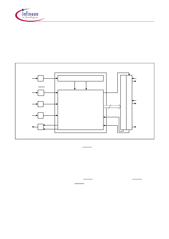
A test access port (TAP) is implemented in the TE3-MUX. The essential part of the TAP
is a finite state machine (16 states) controlling the different operational modes of the
boundary scan. Both, TAP controller and boundary scan, meet the requirements given
by the JTAG standard: IEEE 1149.1.
Figure 22
gives an overview about the TAP
controller.
Figure 22
Block Diagram of Test Access Port and Boundary Scan Unit
If no boundary scan operation is planned TRST has to be connected to V
SS
. TMS and
TDI do not need to be connected since pull- up transistors ensure high input levels in this
case. Nevertheless it would be a good practice to put the unused inputs to defined levels.
In this case, if the JTAG is not used:
TMS = TCK = ‘1’ is recommended.
Test handling (boundary scan operation) is performed via the pins TCK (Test Clock),
TMS (Test Mode Select), TDI (Test Data Input) and TDO (Test Data Output) when the
TAP controller is not in its reset state, i. e. TRST is connected to
V
DD3
or TRST input is
open in which case internal pull sets TRST to
V
DD3
. Test data at TDI are loaded with a
clock signal connected to TCK. ‘1’ or ‘0’ on TMS causes a transition from one controller
state to another; constant ‘1’ on TMS leads to normal operation of the chip.
An input pin (I) uses one boundary scan cell (data in), an output pin (O) uses two cells
(data out, enable) and an I/O-pin (I/O) uses three cells (data in, data out, enable). Note
that most functional output and input pins of the TE3-MUX are tested as I/O pins in
boundary scan, hence using three cells. The boundary scan unit of the TE3-MUX
Clock Generation
Test Access Port (TAP)
TAP Controller
- Finite State Machine
- Instruction Register (4 bit)
- Test Signal Generator
CLOCK
TCK
TRST
TMS
Reset
Data in
TDI
Test
Control
TDO
Enable
Data out
CLOCK
I
B
Control
ID Data out
SS Data
out
n
.
.
.
.
.
.
1
2
Pins
相關(guān)PDF資料 |
PDF描述 |
|---|---|
| TEA1085 | Listening-in circuit for line-powered telephone sets |
| TEA1085A | Listening-in circuit for line-powered telephone sets |
| TEA1085AT | Listening-in circuit for line-powered telephone sets |
| TEA1085T | Listening-in circuit for line-powered telephone sets |
| TEA1093 | Hands-free IC |
相關(guān)代理商/技術(shù)參數(shù) |
參數(shù)描述 |
|---|---|
| TE3Q0TREB2201G | 制造商:Vishay Dale 功能描述:IND FLTR WW 2.2K UH 2% TRD - Bulk |
| TE3Q0TRPJ1000J | 制造商:Vishay Angstrohm 功能描述:Ind Filter Toroid 100uH 5% RDL Bulk 制造商:Vishay Dale 功能描述:IND FLTR WW 100UH 5% TRD - Bulk |
| TE3Q0TRPJ1100J | 制造商:Vishay Dale 功能描述:TE-3Q0TR 110 5% P09 - Bulk |
| TE3Q0TRPJ2201G | 制造商:Vishay Dale 功能描述:IND FLTR WW 2.2K UH 2% TRD - Bulk |
發(fā)布緊急采購(gòu),3分鐘左右您將得到回復(fù)。