- 您現(xiàn)在的位置:買賣IC網(wǎng) > PDF目錄98081 > SII3512ECTU128 PCI BUS CONTROLLER, PQFP128 PDF資料下載
參數(shù)資料
| 型號: | SII3512ECTU128 |
| 元件分類: | 總線控制器 |
| 英文描述: | PCI BUS CONTROLLER, PQFP128 |
| 封裝: | LEAD FREE, TQFP-128 |
| 文件頁數(shù): | 71/132頁 |
| 文件大小: | 3011K |
| 代理商: | SII3512ECTU128 |
第1頁第2頁第3頁第4頁第5頁第6頁第7頁第8頁第9頁第10頁第11頁第12頁第13頁第14頁第15頁第16頁第17頁第18頁第19頁第20頁第21頁第22頁第23頁第24頁第25頁第26頁第27頁第28頁第29頁第30頁第31頁第32頁第33頁第34頁第35頁第36頁第37頁第38頁第39頁第40頁第41頁第42頁第43頁第44頁第45頁第46頁第47頁第48頁第49頁第50頁第51頁第52頁第53頁第54頁第55頁第56頁第57頁第58頁第59頁第60頁第61頁第62頁第63頁第64頁第65頁第66頁第67頁第68頁第69頁第70頁當前第71頁第72頁第73頁第74頁第75頁第76頁第77頁第78頁第79頁第80頁第81頁第82頁第83頁第84頁第85頁第86頁第87頁第88頁第89頁第90頁第91頁第92頁第93頁第94頁第95頁第96頁第97頁第98頁第99頁第100頁第101頁第102頁第103頁第104頁第105頁第106頁第107頁第108頁第109頁第110頁第111頁第112頁第113頁第114頁第115頁第116頁第117頁第118頁第119頁第120頁第121頁第122頁第123頁第124頁第125頁第126頁第127頁第128頁第129頁第130頁第131頁第132頁
SiI3512 PCI to Serial ATA Controller
Data Sheet
Silicon Image, Inc.
DS-0102-D01
2007-2010 Silicon Image, Inc. All rights reserved.
35
CONFIDENTIAL
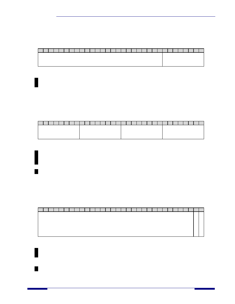
Capabilities Pointer
Address Offset: 0x34
Access Type: Read
Reset Value: 0x0000_0060
31 30 29 28 27 26 25 24 23 22 21 20 19 18 17 16 15 14 13 12 11 10 09 08 07 06 05 04 03 02 01 00
Reserved
Capabilities Pointer
This register defines the link to a list of new capabilities associated with the PCI bus. The register bits are defined below.
Bit [31:08]: Reserved (R). This bit field is reserved and returns zeros on a read.
Bit [07:00]: Capabilities Pointer (R) – Capabilities Pointer. This bit field defaults to 0x60 to define the address for
the 1
st entry in a list of PCI Power Management capabilities.
Max Latency – Min Grant – Interrupt Pin – Interrupt Line
Address Offset: 0x3C
Access Type: Read/Write
Reset Value: 0x0000_0100
31 30 29 28 27 26 25 24 23 22 21 20 19 18 17 16 15 14 13 12 11 10 09 08 07 06 05 04 03 02 01 00
Max Latency
Min Grant
Interrupt Pin
Interrupt Line
This register defines the various control functions associated with the PCI bus. The register bits are defined below.
Bit [31:24]: Max Latency (R) – Maximum Latency. This bit field is hardwired to 0x00.
Bit [23:16]: Min Grant (R) – Minimum Grant. This bit field is hardwired to 0x00.
Bit [15:08]: Interrupt Pin (R) – Interrupt Pin Used. This bit field is hardwired to 0x01 to indicate that the SiI3512
controller uses the INTA# interrupt.
Bit [07:00]: Interrupt Line (R/W) – Interrupt Line. This bit field is used by the system to indicate interrupt line
routing information. The SiI3512 device does not use this information.
Configuration
Address Offset: 0x40
Access Type: Read/Write
Reset Value: 0x0000_0000
31 30 29 28 27 26 25 24 23 22 21 20 19 18 17 16 15 14 13 12 11 10 09 08 07 06 05 04 03 02 01 00
Reserved
B
A5
In
d
Ac
c
E
n
a
P
CI
Hd
r
Wr
E
n
a
This register defines the various control functions associated with the PCI bus. The register bits are defined below.
Bit [31:02]: Reserved (R). This bit field is hardwired to 0x00000000.
Bit [01]: BA5 Ind Acc Ena (R/W) – BA5 Indirect Access Enable. This bit is set to enable indirect access to BA5
address space using Configuration Space registers 0xC0 and 0xC4 (BA5 Indirect Address and BA5 Indirect
Access).
Bit [00]: PCI Hdr Wr Ena (R/W) – PCI Configuration Header Write Enable. This bit is set to enable write access
to the following registers in the PCI Configuration Header: Device ID (0x03–0x02), PCI Class Code (0x09–
0x0B), Subsystem Vendor ID (0x2D–0x2C), and Subsystem ID (0x2F–0x2E).
相關PDF資料 |
PDF描述 |
|---|---|
| SII3531ACNU | PCI BUS CONTROLLER, QCC48 |
| SIO10N268-NU | MULTIFUNCTION PERIPHERAL, PQFP128 |
| SIS300 | GRAPHICS PROCESSOR, PBGA365 |
| SK12430PJT | 800 MHz, OTHER CLOCK GENERATOR, PQCC28 |
| SK12439PJ | 800 MHz, OTHER CLOCK GENERATOR, PQCC28 |
相關代理商/技術參數(shù) |
參數(shù)描述 |
|---|---|
| SII3531 | 制造商:SILICONIMAGE 制造商全稱:SILICONIMAGE 功能描述:SteelVine⑩ Host Controller |
| SII3531A | 制造商:SILICONIMAGE 制造商全稱:SILICONIMAGE 功能描述:PCI Express to Serial ATA Controller |
| SII3531ACNU | 制造商:Silicon Image Inc 功能描述:PCI Express to Serial ATA Controller 48-Pin QFN EP |
| SII3611 | 制造商:SILICONIMAGE 制造商全稱:SILICONIMAGE 功能描述:SATALink Device Bridge |
| SII3611CT80-1.5 | 制造商:SILICON IMAGE 功能描述:3611CT80-1.5 |
發(fā)布緊急采購,3分鐘左右您將得到回復。