- 您現(xiàn)在的位置:買賣IC網(wǎng) > PDF目錄383804 > SCANPSC110FSC (FAIRCHILD SEMICONDUCTOR CORP) SCAN Bridge Hierarchical and Multidrop Addressable JTAG Port (IEEE1149.1 System Test Support) PDF資料下載
參數(shù)資料
| 型號: | SCANPSC110FSC |
| 廠商: | FAIRCHILD SEMICONDUCTOR CORP |
| 元件分類: | 微控制器/微處理器 |
| 英文描述: | SCAN Bridge Hierarchical and Multidrop Addressable JTAG Port (IEEE1149.1 System Test Support) |
| 中文描述: | SPECIALTY MICROPROCESSOR CIRCUIT, PDSO28 |
| 封裝: | 0.300 INCH, MS-013, SOIC-28 |
| 文件頁數(shù): | 13/25頁 |
| 文件大?。?/td> | 283K |
| 代理商: | SCANPSC110FSC |
13
www.fairchildsemi.com
S
Level 2 Protocol
(Continued)
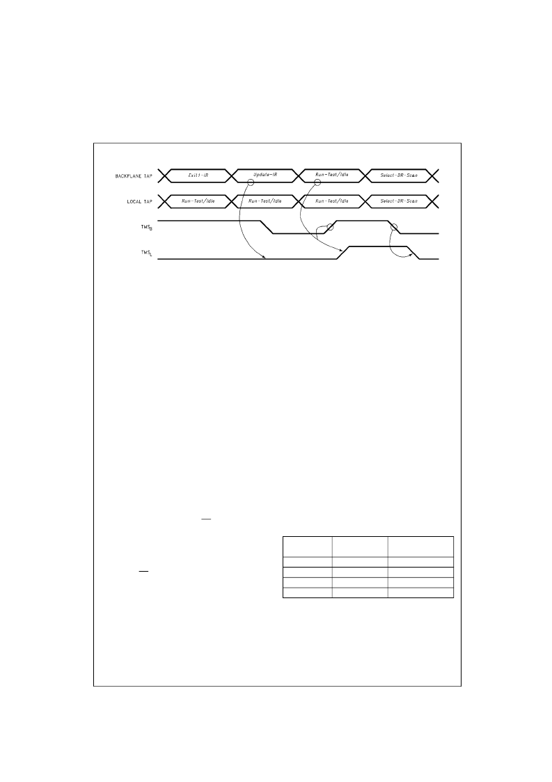
FIGURE 10. Local Scan Port Synchronization from
Parked-RTI
State
Register Descriptions
Instruction Register
The instruction shift register is an 8-bit register that is in
series with the scan chain whenever the TAP Controller of
the SCANPSC110F Bridge is in the
Shift-IR
state. Upon
exiting the
Capture-IR
state, the value
“
XXXXXX01
”
is cap-
tured into the instruction register, where
“
XXXXXX
”
repre-
sents the value on the S
(0
–
5)
inputs.
When the SCANPSC110F controller is in the
Wait-For-
Address
state, the instruction register is used for
SCANPSC110F selection via address matching. In
addressing individual SCANPSC110Fs, the chip
’
s address-
ing logic performs a comparison between a statically-con-
figured (hard-wired) value on that SCANPSC110F
’
s slot
inputs, and an address which is scanned into the chip
’
s
instruction register. Binary address codes
“
000000
”
through
“
111010
”
(
“
00
”
through
“
3A
”
Hex) are reserved for
addressing individual SCANPSC110Fs. Address
“
3B
”
Hex
is for Broadcast mode.
In doing multi-cast (group) addressing, a scanned-in
address is compared against the (previously scanned-in)
contents of a SCANPSC110F's Multi-Cast Group register.
Binary address codes
“
111110
”
through
“
111111
”
(
“
3A
”
through
“
3F
”
Hex) are reserved for multi-cast addressing,
and should not be assigned as SCANPSC110F slot-input
values.
Boundary-Scan Register
The boundary-scan register is a
“
sample only
”
shift register
containing cells from the S
(0
–
5)
and OE inputs. The register
allows testing of circuitry external to the SCANPSC110F. It
permits the signals flowing between the system pins to be
sampled and examined without interfering with the opera-
tion of the on-chip system logic.
The scan chain is arranged as follows:
TDI
B
→
OE
→
S
5
→
S
4
→
S
3
→
S
2
→
S
1
→
S
0
→
LSPN
→
TDO
B
Bypass Register
The bypass register is a 1-bit register that operates as
specified in IEEE Std. 1149.1 once the SCANPSC110F has
been selected. The register provides a minimum length
serial path for the movement of test data between TDI
B
and the LSPN. This path can be selected when no other
test data register needs to be accessed during a board-
level test operation. Use of the bypass register shortens
the serial access-path to test data registers located in other
components on a board-level test data path.
Multi-Cast Group Register
“
Multi-cast
”
is a method of simultaneously communicating
with more than one selected SCANPSC110F.
The multi-cast group register (MCGR) is a 2-bit register
used to determine which multi-cast group a particular
SCANPSC110F is assigned to. Four addresses are
reserved
for
multi-cast
SCANPSC110F is in the
Wait-For-Address
state and
receives a multi-cast address, and if that SCANPSC110F's
MCGR contains a matching value for that multi-cast
address, the SCANPSC110F becomes selected and is
ready to receive Level 2 Protocol (i.e., further instructions).
The MCGR is initialized to
“
00
”
upon entering the
Test-
Logic-Reset
state.
The following actions are used to perform multi-cast
addressing:
1. Assign all target SCANPSC110Fs to a multi-cast group
by writing each individual target SCANPSC110F's
MCGR with the same multi-cast group code (see Table
6). This configuration step must be done by individually
addressing each target SCANPSC110F, using that
chip's assigned slot value.
2. Scan out the multi-cast group address through the
TDI
B
input of
all
SCANPSC110Fs. Note that this occurs
in parallel, resulting in the selection of only those
SCANPSC110Fs whose MCGR was previously pro-
grammed with the matching multi-cast group code.
addressing.
When
a
TABLE 6. Multi-Cast Group Register Addressing
MCGR
Bits 1, 0
00
01
10
11
Hex Address
Binary Address
3C
3D
3E
3F
XX111100
XX111101
XX111110
XX111111
相關(guān)PDF資料 |
PDF描述 |
|---|---|
| SCP-5453 | SOCKET,IC,16PIN,MACHINE TOOLED WIRE WRAP,0.3"WIDE,0.515"LEAD |
| SCP-6122 | POWER OPERATIONAL AMPLIFIER |
| SCS152 | HM Series Hermetically Sealed Basic Switch, Single Pole Double Throw Circuitry, 0.5 A at 28 Vdc, Integral Lever Actuator, Solder Termination |
| SCS152-IS | Small glass bead with axial leads |
| SCS152-IW | Small glass bead with axial leads |
相關(guān)代理商/技術(shù)參數(shù) |
參數(shù)描述 |
|---|---|
| SCANPSC110FSCX | 功能描述:特定功能邏輯 SCAN JTAG Port RoHS:否 制造商:Texas Instruments 產(chǎn)品: 系列:SN74ABTH18502A 工作電源電壓:5 V 封裝 / 箱體:LQFP-64 封裝:Tube |
| SCANSTA101 | 制造商:NSC 制造商全稱:National Semiconductor 功能描述:Low Voltage IEEE 1149.1 STA Master |
| SCANSTA101_06 | 制造商:NSC 制造商全稱:National Semiconductor 功能描述:Low Voltage IEEE 1149.1 STA Master |
| SCANSTA101SM | 功能描述:接口 - 專用 RoHS:否 制造商:Texas Instruments 產(chǎn)品類型:1080p60 Image Sensor Receiver 工作電源電壓:1.8 V 電源電流:89 mA 最大功率耗散: 最大工作溫度:+ 85 C 安裝風(fēng)格:SMD/SMT 封裝 / 箱體:BGA-59 |
| SCANSTA101SM/NOPB | 功能描述:接口 - 專用 Low Vltg IEEE 1149.1 Sys Test Access RoHS:否 制造商:Texas Instruments 產(chǎn)品類型:1080p60 Image Sensor Receiver 工作電源電壓:1.8 V 電源電流:89 mA 最大功率耗散: 最大工作溫度:+ 85 C 安裝風(fēng)格:SMD/SMT 封裝 / 箱體:BGA-59 |
發(fā)布緊急采購,3分鐘左右您將得到回復(fù)。