- 您現(xiàn)在的位置:買賣IC網(wǎng) > PDF目錄383723 > OR3TP12-6BA352I Quad 2.3V 10 MHz OP, I temp, -40C to +85C, 14-TSSOP, TUBE PDF資料下載
參數(shù)資料
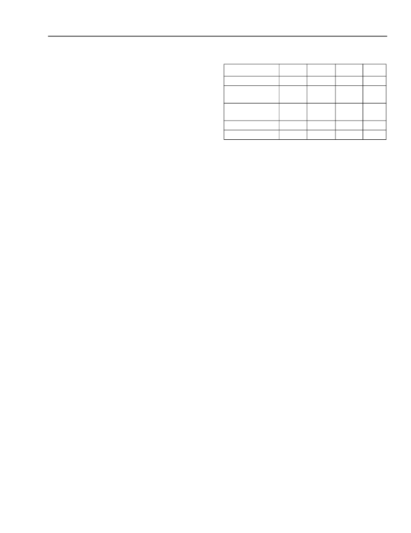
| 型號(hào): | OR3TP12-6BA352I |
| 英文描述: | Quad 2.3V 10 MHz OP, I temp, -40C to +85C, 14-TSSOP, TUBE |
| 中文描述: | 用戶可編程ASIC的特殊功能 |
| 文件頁數(shù): | 17/128頁 |
| 文件大?。?/td> | 2450K |
| 代理商: | OR3TP12-6BA352I |
第1頁第2頁第3頁第4頁第5頁第6頁第7頁第8頁第9頁第10頁第11頁第12頁第13頁第14頁第15頁第16頁當(dāng)前第17頁第18頁第19頁第20頁第21頁第22頁第23頁第24頁第25頁第26頁第27頁第28頁第29頁第30頁第31頁第32頁第33頁第34頁第35頁第36頁第37頁第38頁第39頁第40頁第41頁第42頁第43頁第44頁第45頁第46頁第47頁第48頁第49頁第50頁第51頁第52頁第53頁第54頁第55頁第56頁第57頁第58頁第59頁第60頁第61頁第62頁第63頁第64頁第65頁第66頁第67頁第68頁第69頁第70頁第71頁第72頁第73頁第74頁第75頁第76頁第77頁第78頁第79頁第80頁第81頁第82頁第83頁第84頁第85頁第86頁第87頁第88頁第89頁第90頁第91頁第92頁第93頁第94頁第95頁第96頁第97頁第98頁第99頁第100頁第101頁第102頁第103頁第104頁第105頁第106頁第107頁第108頁第109頁第110頁第111頁第112頁第113頁第114頁第115頁第116頁第117頁第118頁第119頁第120頁第121頁第122頁第123頁第124頁第125頁第126頁第127頁第128頁
Lucent Technologies Inc.
Lucent Technologies Inc.
17
Data Sheet
March 2000
ORCA OR3TP12 FPSC
Embedded Master/Target PCI Interface
PCI Bus Core Detailed Description
(continued)
Parity
The PCI bus core implements all required and optional
features, including the following:
I
Master generates parity on all addresses placed on
the bus.
I
Sending agent generates parity on all data placed on
the bus.
I
Target calculates parity on all addresses received
from the bus.
I
Receiving agent calculates parity on all data
received from the bus.
I
The detected parity error bit in the status register is
set whenever an agent calculates corrupted parity.
I
The signal
perrn
is generated whenever an agent
calculates corrupted data parity and the parity error
response bit is set in the PCI command register.
I
The signal
serrn
is generated whenever an agent
calculates a corrupt address parity.
66 MHz Operation
The PCI bus core is fully compliant to PCI Specification
requirements at all clock rates up to 66 MHz. All
33 MHz requirements are also met.
Timing Budget
The PCI bus core’s timing budget is summarized in
Table 4. Note that the 66 MHz timing requirements only
allow 5 ns for signal proagation (T
PROP
), as compared
to 10 ns at 33 MHz. The effect of the reduction is to
reduce also the number of agents that the bus can sup-
port, although the actual number is not specified in the
PCI Specification and is dependent on the design of
the hardware components. The four components of the
timing budget are T
VAL
(valid output delay), T
PROP
(propagation time), T
SU
(input setup time), and T
SKEW
(clock skew); of these, only T
VAL
and T
SU
are controlled
by the PCI component, and T
PROP
and T
SKEW
are sys-
tem parameters. Table 4 includes a third column (also
shown in the PCI Specification); this column indicates
the performance attainable if all 66 MHz requirements
are met except T
PROP
= 10 ns, which is the 33 MHz
value. In this case, the total budget increases from
15 ns (66 MHz) to 20 ns (50 MHz).
Table 4. Timing Budgets
64-Bit Addressing
The PCI bus core fully supports 64-bit addressing,
whether or not the PCI bus core is configured to utilize
the 64-bit data extension. When the PCI bus core is a
64-bit Target being addressed by 64-bit Master, the PCI
bus core will decode the address one cycle faster so
that dual-address operation will have no performance
impact; see PCI Specification 2.1, Section 3.10.1 for
details.
Section 3.10.1 of the PCI Specification 2.1 also states
that a Master that supports 64-bit addressing must
nevertheless generate requests utilizing a single
address instead of a dual-address when the upper
32 bits are all zeros. This shortens the request time by
one cycle when communicating with 32-bit Targets.
FIFO Memories and Control
The OR3TP12 embedded core contains four FIFO
memories and supporting control logic. Two FIFOs are
for the Master FIFO interface data and two for the Tar-
get FIFO interface data. These FIFOs are configured to
operate in 64-bit mode and can also carry byte enable
bits on a per-byte basis (e.g., a 64-bit FIFO actually
carries 64 bits of data and eight byte enable bits for a
total of 72 bits). All FIFOs have two relevant flags which
extend into the FPGA logic for user application (e.g., a
Target read FIFO on the FPGA side has Full and Full-4
flags extending into the FPGA logic). Clocking for the
FPGA port of all FIFOs is flexible, with options for dif-
ferent clocks for the Master and Target FIFOs, all
sourced by the FPGA logic.
Timing Element 33 MHz 50 MHz 66 MHz
Cycle Time
30.0
Valid Output
Delay
Propagation
Time
Input Setup Time
7.0
Clock Skew
2.0
Unit
ns
ns
20.0
7.5
15.0
6.0
11.0
10.0
6.5
5.0
ns
4.5
1.5
3.0
1.0
ns
ns
相關(guān)PDF資料 |
PDF描述 |
|---|---|
| OR3TP12-6PS240 | Single 2.3V 10 MHZ OP, -40C to +125C, 14-SOIC 150mil, T/R |
| OR3TP12-6PS240I | Quad 2.3V 10 MHz OP, I temp, -40C to +85C, 14-SOIC 150mil, T/R |
| OR3TP12 | Field-Programmable System Chip (FPSC) Embedded Master/Target PCI Interface |
| OR62 | OR62 is a 6-input OR gate with 2x drive strength |
| OR73 | 7-input OR gate with 3x drive strength. |
相關(guān)代理商/技術(shù)參數(shù) |
參數(shù)描述 |
|---|---|
| OR3TP126BAN256-DB | 制造商:Lattice Semiconductor Corporation 功能描述: |
| OR3TP12-6PS240 | 制造商:未知廠家 制造商全稱:未知廠家 功能描述:User Programmable Special Function ASIC |
| OR3TP12-6PS240I | 制造商:未知廠家 制造商全稱:未知廠家 功能描述:User Programmable Special Function ASIC |
| OR3TP127BA256-DB | 功能描述:FPGA - 現(xiàn)場可編程門陣列 2016 LUT 187 I/O RoHS:否 制造商:Altera Corporation 系列:Cyclone V E 柵極數(shù)量: 邏輯塊數(shù)量:943 內(nèi)嵌式塊RAM - EBR:1956 kbit 輸入/輸出端數(shù)量:128 最大工作頻率:800 MHz 工作電源電壓:1.1 V 最大工作溫度:+ 70 C 安裝風(fēng)格:SMD/SMT 封裝 / 箱體:FBGA-256 |
| OR3TP127BA352-DB | 功能描述:FPGA - 現(xiàn)場可編程門陣列 2016 LUT 187 I/O RoHS:否 制造商:Altera Corporation 系列:Cyclone V E 柵極數(shù)量: 邏輯塊數(shù)量:943 內(nèi)嵌式塊RAM - EBR:1956 kbit 輸入/輸出端數(shù)量:128 最大工作頻率:800 MHz 工作電源電壓:1.1 V 最大工作溫度:+ 70 C 安裝風(fēng)格:SMD/SMT 封裝 / 箱體:FBGA-256 |
發(fā)布緊急采購,3分鐘左右您將得到回復(fù)。