- 您現(xiàn)在的位置:買賣IC網(wǎng) > PDF目錄384759 > MT90221AL (Mitel Networks Corporation) Quad IMA/UNI PHY Device PDF資料下載
參數(shù)資料
| 型號(hào): | MT90221AL |
| 廠商: | Mitel Networks Corporation |
| 英文描述: | Quad IMA/UNI PHY Device |
| 中文描述: | 四IMA的/單向物理層設(shè)備 |
| 文件頁數(shù): | 36/114頁 |
| 文件大?。?/td> | 304K |
| 代理商: | MT90221AL |
第1頁第2頁第3頁第4頁第5頁第6頁第7頁第8頁第9頁第10頁第11頁第12頁第13頁第14頁第15頁第16頁第17頁第18頁第19頁第20頁第21頁第22頁第23頁第24頁第25頁第26頁第27頁第28頁第29頁第30頁第31頁第32頁第33頁第34頁第35頁當(dāng)前第36頁第37頁第38頁第39頁第40頁第41頁第42頁第43頁第44頁第45頁第46頁第47頁第48頁第49頁第50頁第51頁第52頁第53頁第54頁第55頁第56頁第57頁第58頁第59頁第60頁第61頁第62頁第63頁第64頁第65頁第66頁第67頁第68頁第69頁第70頁第71頁第72頁第73頁第74頁第75頁第76頁第77頁第78頁第79頁第80頁第81頁第82頁第83頁第84頁第85頁第86頁第87頁第88頁第89頁第90頁第91頁第92頁第93頁第94頁第95頁第96頁第97頁第98頁第99頁第100頁第101頁第102頁第103頁第104頁第105頁第106頁第107頁第108頁第109頁第110頁第111頁第112頁第113頁第114頁
MT90221
28
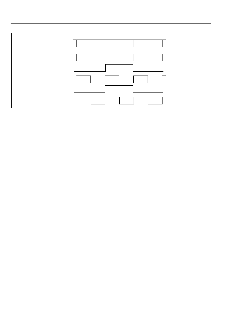
Figure 12 - Mode 1 and 5: Generic PCM Interface for T1
T1 Frame
Bit Cells
at DSTx0-3
bit 193
bit 1
bit 2
...
Serial Bit
Stream
Bit Cell
...
Bit Cell
TXSYNC
RXSYNC
TXCK
RXCK
...
...
...
Unused or
High Impedance
or spaced) are supported. The TXCLK and RXCLK
are 2.048 MHz signal and the TXSYNC and
RXSYNC are a frame pulse of one full bit duration
that occurs at the beginning of the frame. The frame
rate is 8 KHz. The polarity of the TXCK, RXCK,
TXSYNC and RXSYNC and their active edge is
programmable using
TX PCM Link Control
register
number 1 and
RX PCM Link Control
register.
4.2.4
The channel/timeslot mapping in this mode is similar
to the ST-BUS mode for E1. The differences are:
the interface clocks (RXCK and TXCK) operate
at 2.048 MHz only
the synchronization signals (TXSYNC and
RXSYNC) are valid for one clock cycle (488
nsec) during the first bit of the frame
In PCM Mode 3, the TXCK and TXSYNC pins
are defined as outputs.
In PCM Mode 7, the TXCK and TXSYNC are
defined as inputs.
The edge of the RXCK and TXCK signals that is
used to sample the incoming, and transmit the
outgoing, data is fully programmable on a per link
basis. This allows the MT90221 to operate with the
majority of off-the-shelf E1 framers.
Mode 3 and 7: Generic PCM Interface for E1
The MT90221 does not use timeslots 0 and 16 to
perform the G.804 transmission convergence
function (see Figure 13).
4.2.5
TXSYNC Signal in Mode 5 and 7
The TXSYNC signal is defined as an input in PCM
mode 5 and 7 and is sampled at the bit boundary. A
positive delay of 10 nsec is expected between the
TXCLK signal at the bit boundary and the time the
TXSYNC changes This may cause some inter-
operability
problems
when
connected to some off-the-shelf framers as the
TXSYNC can be slightly ahead of the TXCLK signal.
In this case, the TXSYNC signal need to be delayed
to ensure proper operation of the TX PCM port.
the
MT90220
is
4.3
In PCM Modes 2, 4, 5 and 7, the TXCK and TXSYNC
are inputs and are generated by external circuitry.
Clocking Options
In PCM Modes 1, 3, 6 and 8, the TXCK and TXSYNC
are outputs. TXCK source is software selectable and
can be any of the four RXCK signals or four external
REFCK inputs (see Figure 14). The TXSYNC is
generated from the TXCK signal.
The RXCK pins are always defined as inputs and the
proper signal must be provided to each input.
4.3.1
The RXSYNC signal is used to align the incoming
DSTi data to retrieve all the T1 or E1 channels. The
RXSYNC pulse can be present for each PCM frame
(8Khz) or once per Superframe (every 12 or 24 PCM
frames). The period and position of the RXSYNC is
verified for each receive block independently. A status
bit (1 per link) in the
RX Sync Status
register is set if
the synchronization pulse occurs at an unexpected
time in the frame. The RX block will be re-aligned with
this new synchronization pulse.
Verification of the RXSYNC Period
4.3.2
The TXSYNC signal is used to align the outgoing
DSTo data to retrieve all the T1 or E1 channels.
When defined as input, the TXSYNC pulse can be
present for each PCM frame (8Khz) or once per
Superframe (every 12 or 24 PCM frames). The
Verification of the TXSYNC Period
相關(guān)PDF資料 |
PDF描述 |
|---|---|
| MT9041B | T1/E1 System Synchronizer |
| MT9041BP | T1/E1 System Synchronizer |
| MT9041 | Multiple Output Trunk PLL |
| MT9041AP | IC REG LDO 150MA 5.0V 0.5% 8SOIC |
| MT9042C | Multitrunk System Synchronizer |
相關(guān)代理商/技術(shù)參數(shù) |
參數(shù)描述 |
|---|---|
| MT90222 | 制造商:ZARLINK 制造商全稱:Zarlink Semiconductor Inc 功能描述:4/8/16 Port IMA/TC PHY Device |
| MT90222AG | 制造商:Microsemi Corporation 功能描述:ATM IMA 40MBPS 2.5V 384BGA - Trays |
| MT90222AG2 | 制造商:Microsemi Corporation 功能描述:ATM IMA 40MBPS 2.5V 384BGA /BAKE/DRYPACK - Trays |
| MT90223AG | 制造商:Microsemi Corporation 功能描述:ATM IMA 80MBPS 2.5V 384BGA - Trays |
| MT90223AG2 | 制造商:Microsemi Corporation 功能描述:ATM IMA 80MBPS 2.5V 384BGA - Trays |
發(fā)布緊急采購(gòu),3分鐘左右您將得到回復(fù)。